
Use of Si-rich oxide film as a chemical potential barrier for controlled oxidation

a technology of chemical potential barrier and silicide layer, which is applied in the direction of basic electric elements, electrical apparatus, and semiconductor devices, can solve the problems of so-called peeling of silicide layer and reciprocal lifting between layers, dislocation and defect, and short circuit between source and drain region

Inactive Publication Date: 2001-08-14
TEXAS INSTR INC
View PDF4 Cites 33 Cited by
  • Summary
  • Abstract
  • Description
  • Claims
  • Application Information

AI Technical Summary

Benefits of technology

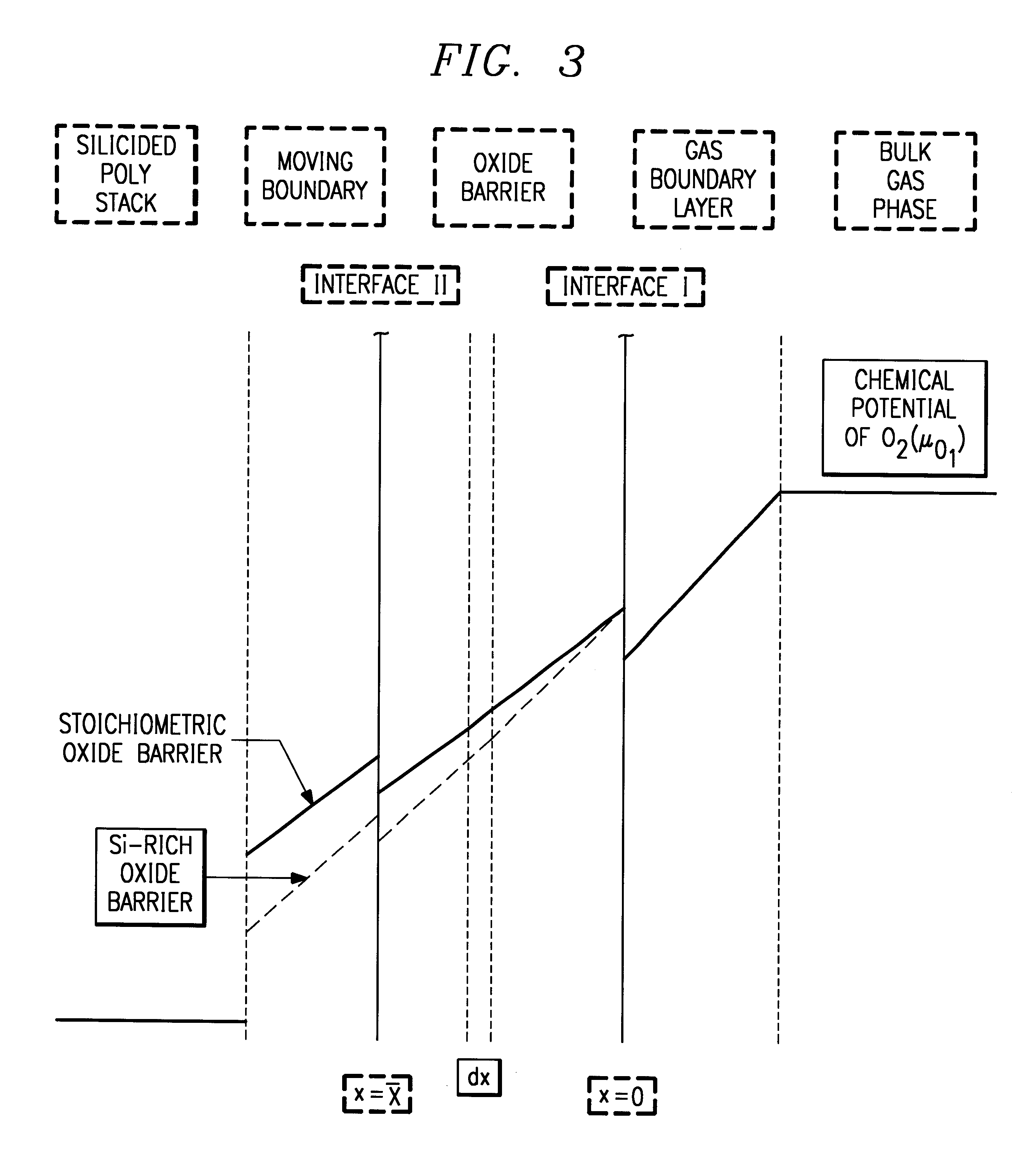
The invention is a two-step oxidation process that provides a preliminary, fast, uniform, and low temperature deposition of a layer of silicon-enriched oxide followed by a reoxidation. The term silicon enriched oxide is used to refer to a silicon oxide layer having an excess of silicon atoms. The silicon-enriched oxide is stable and its composition SiO.sub.x, can be accurately controlled during deposition. The preliminary oxide deposition enables the subsequent thermal oxidation step to be carried out in low pressure conditions and not at extreme temperatures. This assures a precise control of the chemical-physical features of the obtained oxide.

Problems solved by technology

First of all, the oxidation does not uniformly occur on the various layers of the gate stack, thereby causing the so-called peeling of the silicide layer and a reciprocal lifting between layers.
Moreover, when the thermal oxidation step is executed after performing dopant implantations, the dopants diffuse very fast in the substrate crystal lattice till they concentrate, thereby producing dislocations and defects and causing short circuits between the source and drain regions.
Therefore, performing a new thermal oxidation involves severe reliability problems, with resulting degradation of the device quality to a lower level as the one obtainable without a protection oxide layer.
In conclusion, the oxidation according to the prior art to minimize DRL is not feasible due to the high agressiveness of the thermal oxidation.
Consequently, DRL is not effectively minimizable and this implies significant economical losses, because 5% of manufactured devices are not reliable and have to be scrapped.

Method used


Image

  • Use of Si-rich oxide film as a chemical potential barrier for controlled oxidation
  • Use of Si-rich oxide film as a chemical potential barrier for controlled oxidation
  • Use of Si-rich oxide film as a chemical potential barrier for controlled oxidation

Examples


Embodiment Construction

The invention will now be described in conjunction with forming a silicon-rich oxide barrier at the gate level of a FAMOS process. It will be apparent to those of ordinary skill in the art that the use of Si-rich oxide barrier, according to the invention, can be made any device process level where oxygen gettering is required in order to protect the underlying film or device structure while oxidation is required at the overlying structures. For example, the invention may be used as liner layers for controlling etch characteristics or as a means for controlling transistor VTs.

The invention is a two-step oxidation process that provides a preliminary, fast, uniform, and low temperature deposition of a layer of silicon-enriched oxide followed by a reoxidation. The term silicon enriched oxide is used to refer to a silicon oxide layer having an excess of silicon atoms. The silicon-enriched oxide is stable and its composition SiO.sub.x, can be accurately controlled during deposition. The p...


PUM

PropertyMeasurementUnit
temperatureaaaaaaaaaa
refractive indexaaaaaaaaaa

Abstract

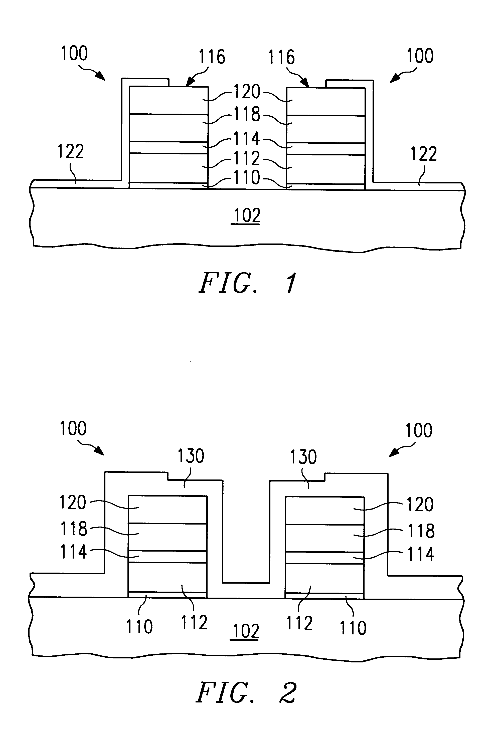
An oxidation process for reducing the data retention loss (DRL) in a FAMOS device comprising the steps of (1) low temperature deposition of a silicon-enriched silicon oxide (130) over a FAMOS transistor gate stack (116) and (2) annealing said silicon-enriched oxide (130) at a high temperature in oxygen atmosphere to convert said silicon-enriched oxide (130) to a thermal oxide. The silicon enriched oxide (130) acts as both an oxygen getter and diffusion barrier during the annealing step.

Description

The invention is generally related to the field of semiconductor processing and more specifically to the use of a Si-rich oxide barrier.It is known that the manufacturing of semiconductor devices comprises a chemical processing consisting of a series of steps in which different elements of the devices to be manufactured are progressively made. The semiconductor mainly used is silicon.Frequently, for silicon devices, one or more steps are required during said chemical processing in which a silicon dioxide should be obtained.This requirement is particularly demanding in manufacturing electrically programmable fast access non volatile memories, so-called "Flash EPROM", that are provided with Floating-Gate-Avalanche-Injection MOS transistors, called "FAMOS", substantially made up of MOS transistors the gate regions of which are insulated.Preferably, said FAMOS transistors include, upon the channel area of the substrate, a structure made up of a stack of different layers, so called gate ...

Claims


Application Information

Patent Timeline
Patent Type & Authority Patents(United States)
IPC IPC(8): H01L21/02H01L21/70H01L21/321H01L21/316H01L21/8247H01L21/314
CPCH01L21/02164H01L21/02211H01L21/02274H01L21/02337H01L21/32105H01L27/11521H01L21/31612Y10S438/971H01L21/31662H10B41/30
Inventor MISRA, SUDHANSHU
Owner TEXAS INSTR INC
Learn More