

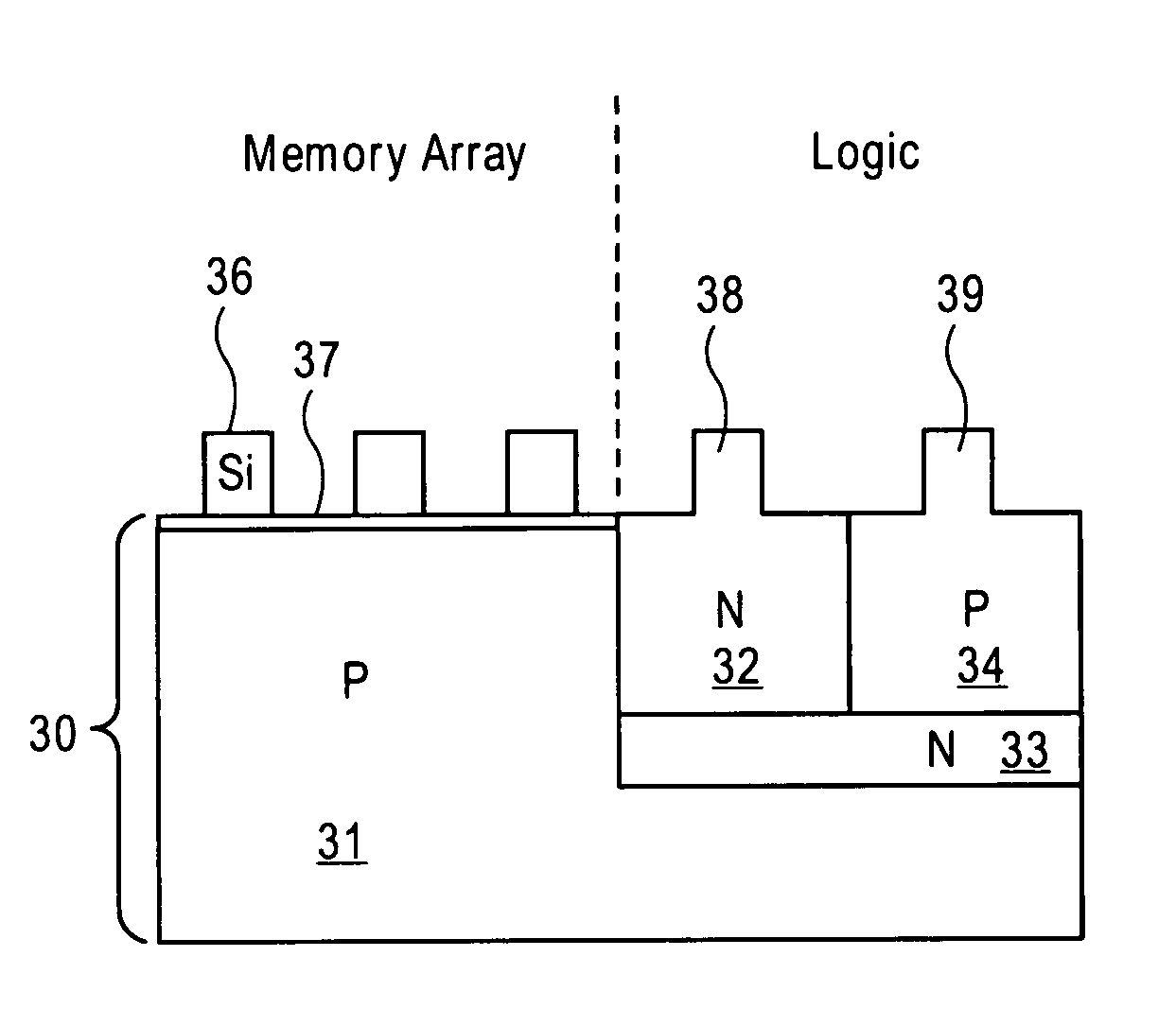
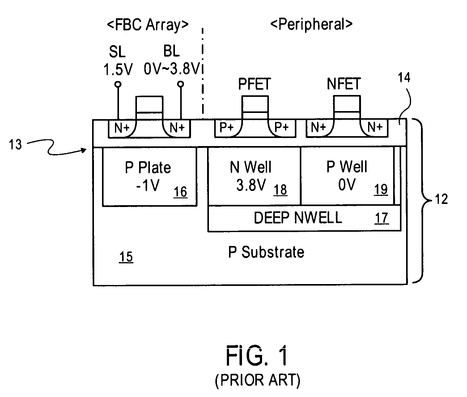
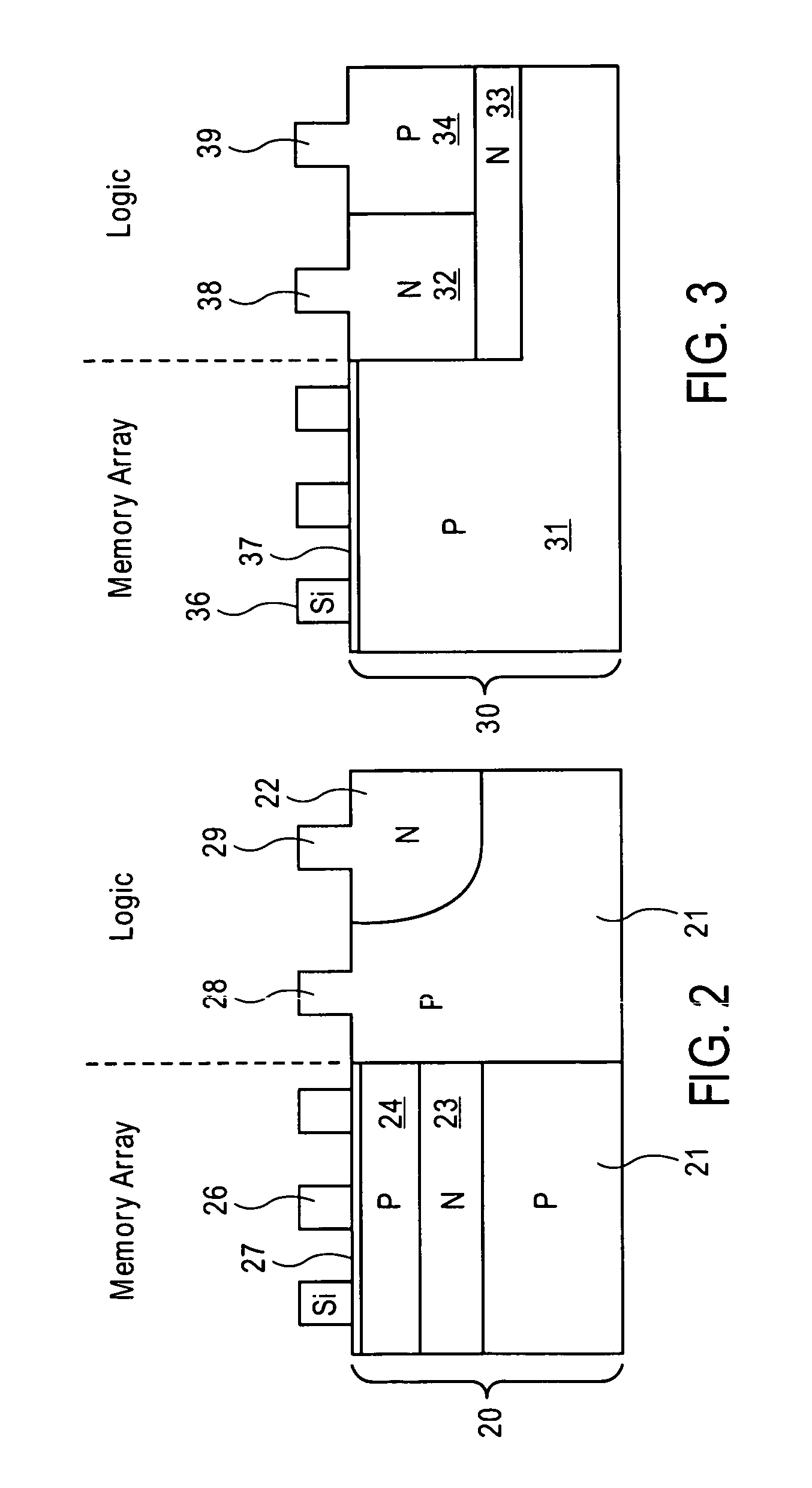
Integration of a floating body memory on SOI with logic transistors on bulk substrate
a floating body memory and logic transistor technology, applied in the direction of basic electric elements, semiconductor devices, electrical equipment, etc., can solve the problems of reducing the performance of logic devices for sufficiently thin boxes, fbc arrays and logic devices are fabricated
- Summary
- Abstract
- Description
- Claims
- Application Information
AI Technical Summary
Problems solved by technology
Method used
Image

Examples
Embodiment Construction
[0017]In the following description, a memory and method for fabricating the memory is described. Numerous specific details are set forth, such as specific conductivity types, to provide a thorough understanding of the present invention. It will be apparent to one skilled in the art, that the present invention may be practiced without these specific details. In other instances, well known processing steps and circuits have not been described in detail, in order not to unnecessarily obscure the present invention.
[0018]Below, reference is made to a silicon-oxide-insulator (SOI) substrate. SOI substrates are well-known in the semiconductor industry. By way of example, they are fabricated by bonding a monocrystalline silicon layer onto a bulk silicon substrate and then planarizing the silicon layer so that it is relatively thin. This relatively thin, low body effect SOI layer is used for active devices. Other techniques are known for forming an SOI substrate including, for instance, impl...
PUM
 Abstract
Description
Claims
Application Information