Semiconductor package with embedded die

Active Publication Date: 2008-05-15
STATS CHIPPAC INC
View PDF25 Cites 92 Cited by
  • Summary
  • Abstract
  • Description
  • Claims
  • Application Information

AI Technical Summary

Benefits of technology

[0009]Prior to forming the circuitry layer, the upper surfaces of the stud bumps can be planarized so that the contact sites of the circuitry layer are substantially coplanar and therefore can form robust connections with bumps or other contacts of the component(s) mounted on the circuitry layer. Another advantage of employing stud bumps for die-level and substrate-level interconnections is that a relatively fine pitch can be achieved. In particular embodiments, the pitch of the substrate-level stud bumps can be about 80 microns or less, and more desirably about 60 microns or less. The pitch of the die-level stu

Problems solved by technology

Conventional chip packing technologies have two inherent limitations: (1) the input/output emerges from only one side of the package (i.e., either from the top or bottom side of the package), and hence integration in both directions along the “z-axis” is difficult, and (2) the footprint of the package is either equal to the die size for fan-in configurations (e.g., WLCSP) or significantly greater than the die size for fan-out configurations.
First, using conventional laser drilling or other known techniques for forming the holes in the encapsulating layer, the pitch between vertical

Method used


Image

  • Semiconductor package with embedded die
  • Semiconductor package with embedded die
  • Semiconductor package with embedded die

Examples


Example

[0024]As used herein, the singular forms “a,”“an,” and “the” refer to one or more than one, unless the context clearly dictates otherwise.

[0025]As used herein, the term “includes” means “comprises.” For example, a device that includes or comprises A and B contains A and B but may optionally contain C or other components other than A and B. A device that includes or comprises A or B may contain A or B or A and B, and optionally one or more other components such as C.

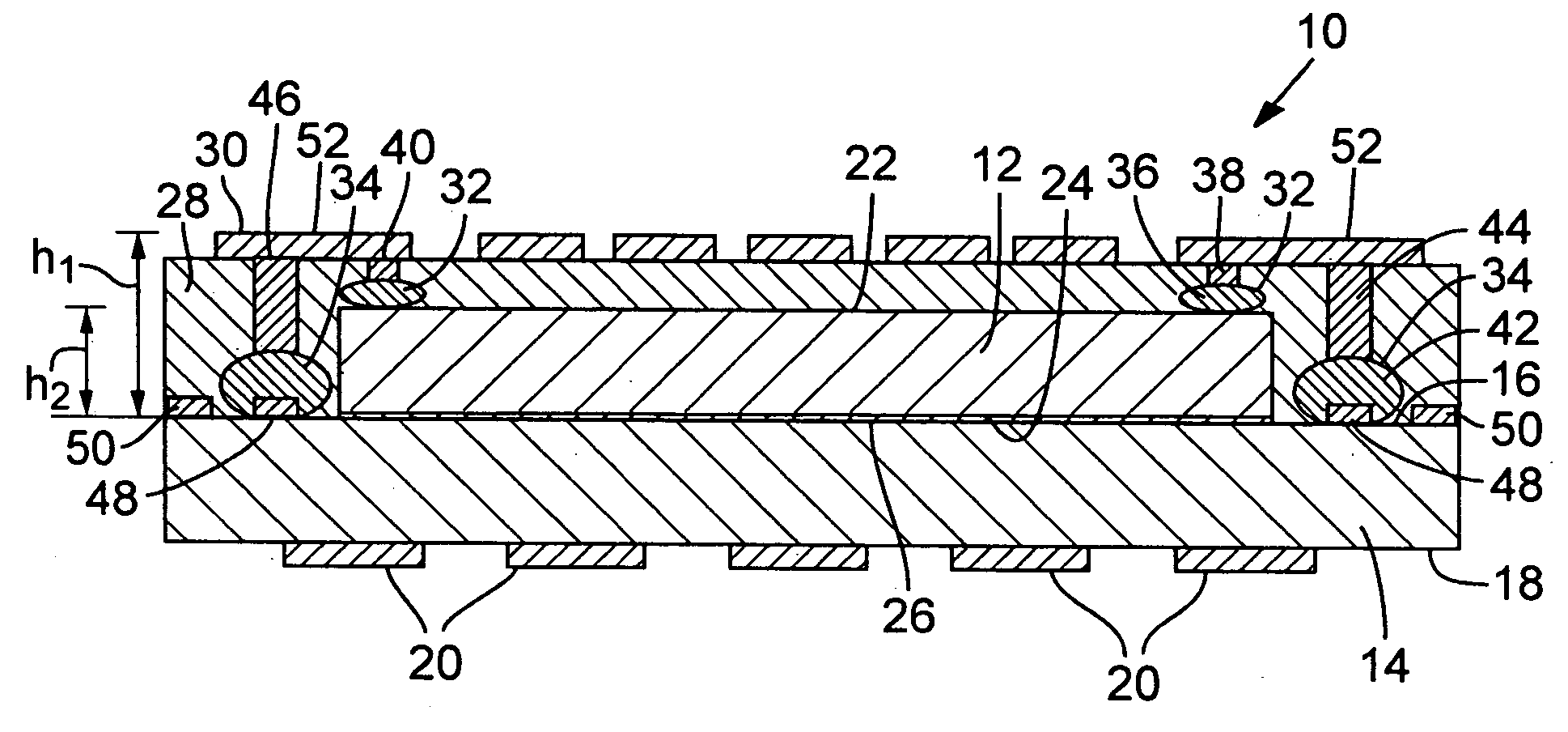
[0026]According to one aspect, the present disclosure concerns embodiments of a semiconductor package employing stud bump interconnections for increased integration in the direction of the z-axis. The semiconductor package can include a die mounted in a face-up configuration (similar to a wire bond package) or in a face-down or flip chip configuration.

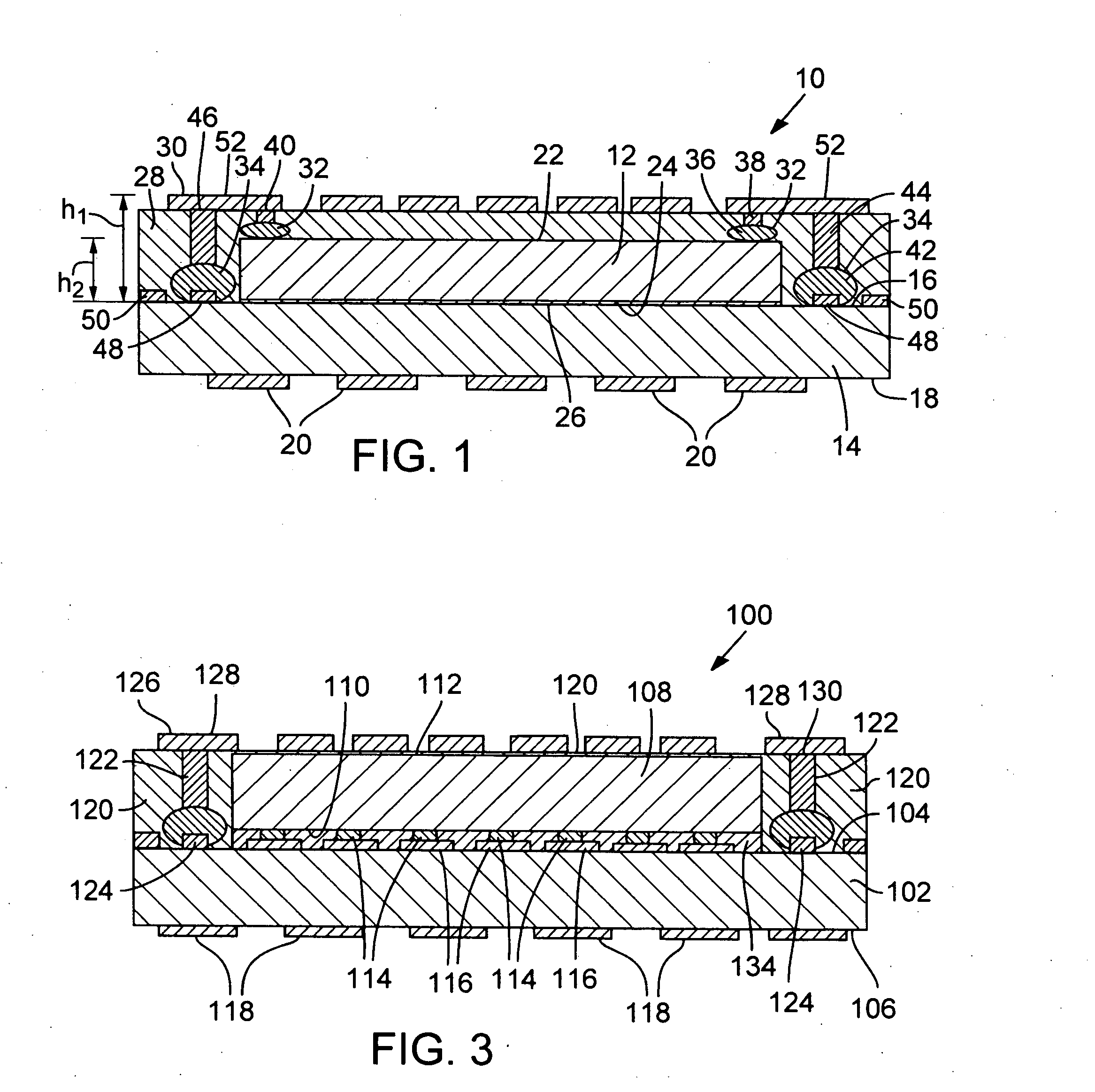
[0027]FIG. 1 shows an exemplary embodiment of semiconductor package 10 including at least one die 12 positioned in a face-up configuration on a substrate 14. The die 12 can ...


PUM


Abstract

A semiconductor package having an embedded die and solid vertical interconnections, such as stud bump interconnections, for increased integration in the direction of the z-axis (i.e., in a direction normal to the circuit side of the die). The semiconductor package can include a die mounted in a face-up configuration (similar to a wire bond package) or in a face-down or flip chip configuration.

Description

FIELD[0001]The present disclosure relates to semiconductor packing.BACKGROUND[0002]Electronic products such as mobile phones, computers and various consumer products require higher semiconductor functionality and performance in a limited footprint and minimal thickness and weight at the lowest cost. This has driven the industry to increase integration on the individual semiconductor chips.[0003]Conventional chip packing technologies have two inherent limitations: (1) the input / output emerges from only one side of the package (i.e., either from the top or bottom side of the package), and hence integration in both directions along the “z-axis” is difficult, and (2) the footprint of the package is either equal to the die size for fan-in configurations (e.g., WLCSP) or significantly greater than the die size for fan-out configurations.[0004]A recent technique for integrating along the z-axis involves encapsulating a die on a substrate, drilling holes through the encapsulating layer arou...

Claims


Application Information

Patent Timeline
IPC IPC(8): H01L23/36H01L23/48H01L21/56
CPCH01L23/3121H01L24/24H01L2924/1461H01L24/82H01L25/105H01L2224/24051H01L2224/24226H01L2924/01012H01L2924/01013H01L2924/01029H01L2924/01042H01L2924/01074H01L2924/01075H01L2924/01079H01L2924/14H01L2924/1433H01L2924/19041H01L2924/01005H01L2924/01006H01L2924/01033H01L2924/014H01L2225/1035H01L21/56H01L23/49811H01L2924/00H01L2924/12042H01L2224/45144H01L2924/00014H01L24/45H01L2224/45015H01L2924/207H01L24/03H01L24/05H01L24/13H01L24/27H01L24/29H01L24/46H01L2224/04042H01L2224/435
Inventor PENDSE, RAJENDRA D.
Owner STATS CHIPPAC INC
Why Eureka
Try Eureka