

Electronic device having liquid crystal polymer solder mask and outer sealing layers, and associated methods
a liquid crystal polymer and solder mask technology, applied in the direction of electrical apparatus construction details, conductive pattern formation, association of printed circuit non-printed electric components, etc., can solve the problems of increased risk of bridging and electrical shorting, solder reflow process, and inability to protect closely spaced pads with solder masks, so as to achieve the effect of attaching an electronic component to a substra
- Summary
- Abstract
- Description
- Claims
- Application Information
AI Technical Summary
Benefits of technology
Problems solved by technology
Method used
Image

Examples
Embodiment Construction
[0019]The present invention will now be described more fully hereinafter with reference to the accompanying drawings, in which preferred embodiments of the invention are shown. This invention may, however, be embodied in many different forms and should not be construed as limited to the embodiments set forth herein. Rather, these embodiments are provided so that this disclosure will be thorough and complete, and will fully convey the scope of the invention to those skilled in the art. Like numbers refer to like elements throughout.
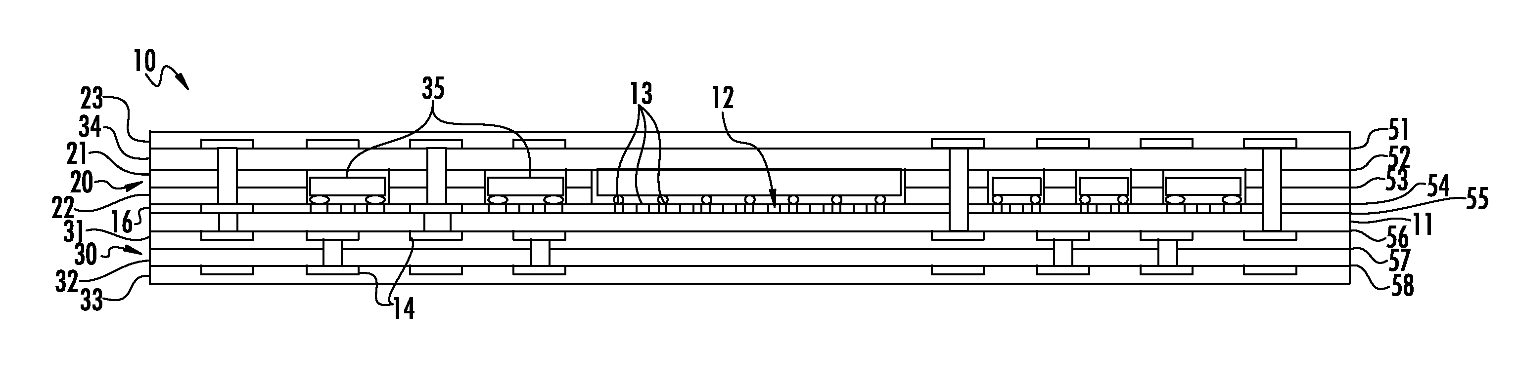
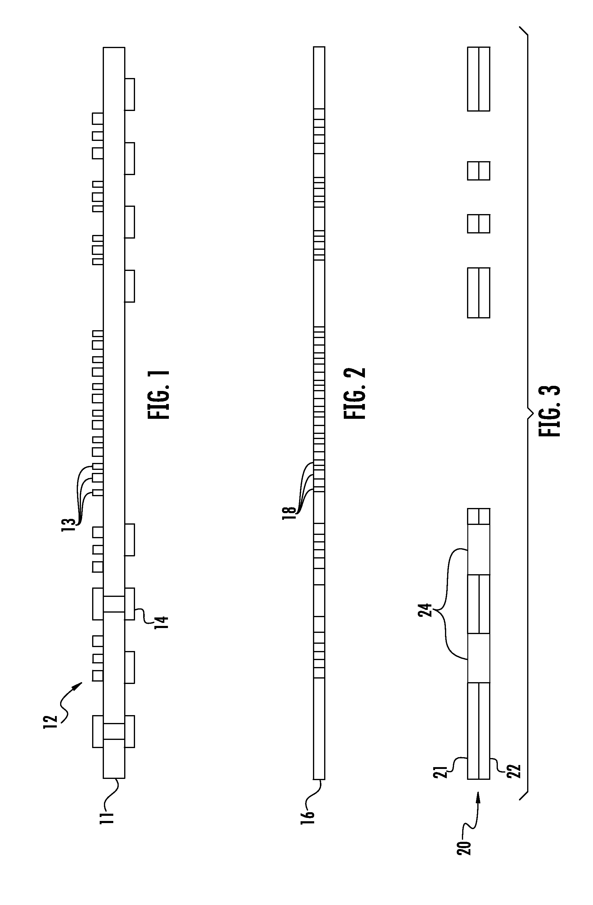
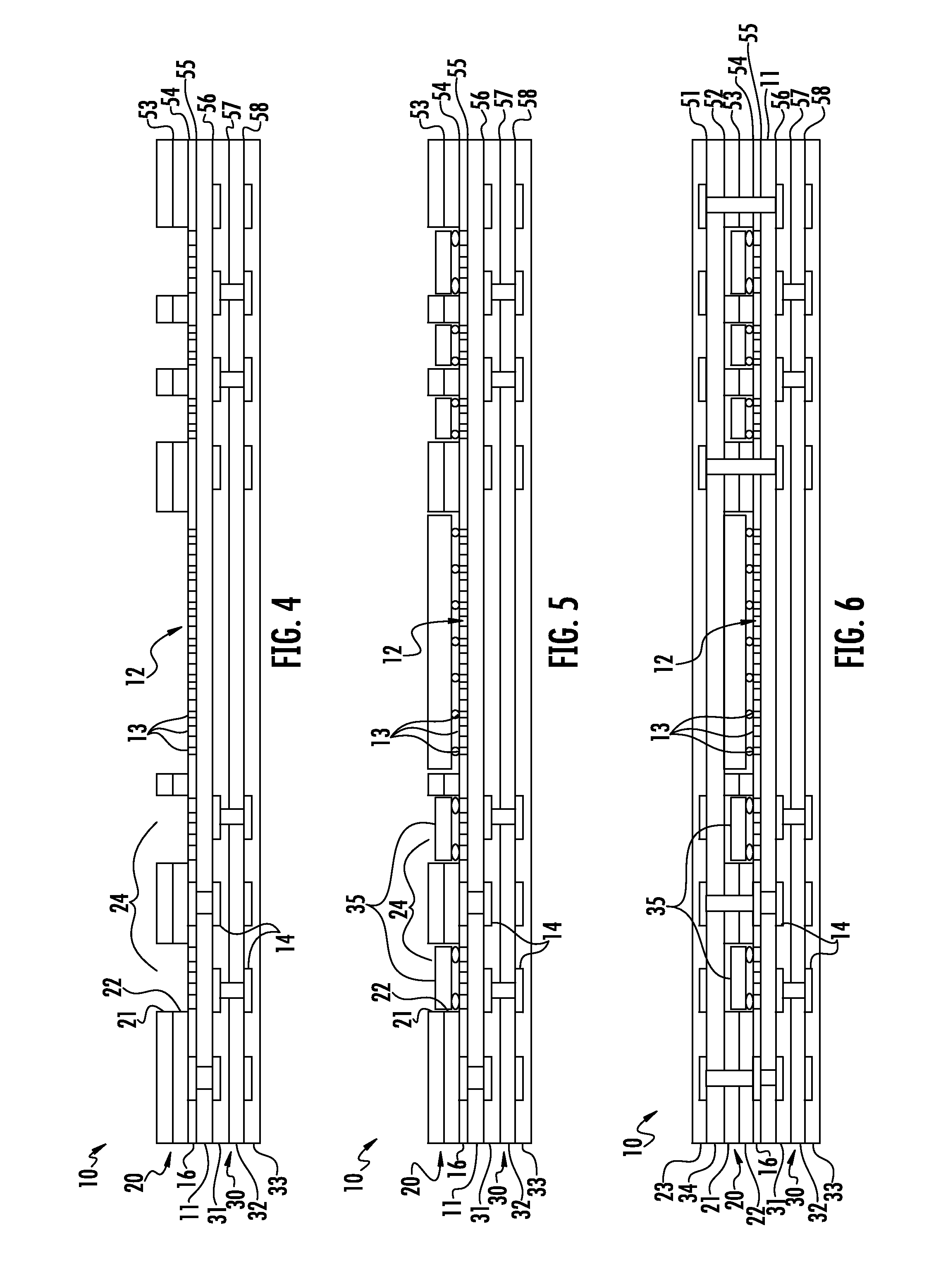
[0020]Referring initially to the flowchart 40 of FIG. 7, together with FIGS. 1-6, a method of making an electronic device 10 is now described. After the start (Block 41), a circuit layer 12 comprising at least one solder pad 13 is formed on a substrate 11 (Block 42), as shown in FIG. 1. Here, the circuit layer 12 illustratively comprises a plurality of solder pads 13 arranged in an array pattern. In addition, electrically conductive vias 14 are formed in t...
PUM
| Property | Measurement | Unit |
|---|---|---|
| dielectric strength | aaaaa | aaaaa |
| dielectric strength | aaaaa | aaaaa |
| dielectric | aaaaa | aaaaa |
Abstract
Description
Claims
Application Information