Fabrication method of space transformer for semiconductor test probe card

A technology of space transformation and testing probes, which is applied in the field of probe cards, can solve problems such as incompatibilities, and achieve the effect of reducing pitch distribution

Active Publication Date: 2010-03-17
TAIWAN SEMICON MFG CO LTD
View PDF0 Cites 18 Cited by
  • Summary
  • Abstract
  • Description
  • Claims
  • Application Information

AI Technical Summary

Problems solved by technology

However, the minimum C4 contact pad pitch of these known space transformers is usually about 150 microns, which cann

Method used


Image

  • Fabrication method of space transformer for semiconductor test probe card
  • Fabrication method of space transformer for semiconductor test probe card
  • Fabrication method of space transformer for semiconductor test probe card

Examples


Embodiment Construction

[0058] In order to make the above-mentioned and other objects, features, and advantages of the present invention more clearly understood, the preferred embodiments are specifically listed below, together with the accompanying drawings, and are described in detail as follows:

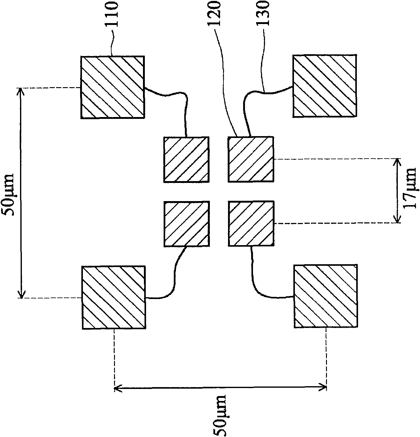
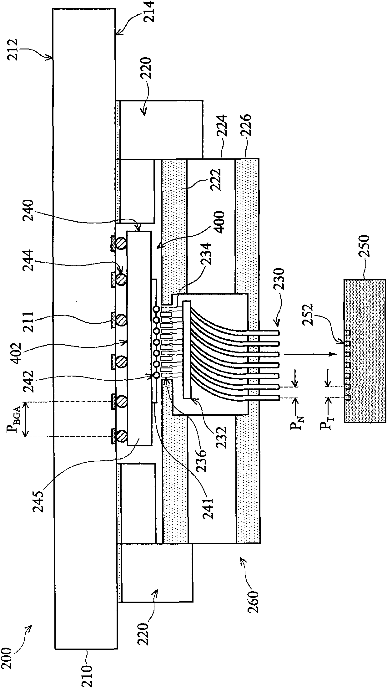
[0059] figure 2 An exemplary embodiment is shown of a commercially available test probe card 200 having a space transformer 240 with fine pitch C4 contact pads that has been modified by the method proposed by the present invention array. The test probe card 200 may be any suitable commercially available test probe card, such as, but not limited to, the Probe with Needle Probes from Wentworth Laboratories, Inc. of Brookfield, CT. card, or from ofLivermore, CA obtained with Probe card for needle probes. The above-mentioned probe card is preferably selected to have a spacing or pitch of 50 microns or less for the test needle-like probes, so as to have the same spacing or spacing as the test pad 110 ...


PUM


Abstract

The invention discloses a space transformer for a semiconductor test probe card and a method of fabrication. The method may include depositing a first metal layer as a ground plane on a space transformer substrate having a plurality of first contact test pads defining a first pitch spacing, depositing a first dielectric layer on the ground plane, forming a plurality of second test contacts defining a second pitch spacing different than, the first pitch spacing, and forming a plurality of redistribution leads on the first dielectric layer to electrically couple the first contact test pads to the second contact test pads. In some embodiments, the redistribution leads may be built directly on the space transformer substrate. The method may be used in one embodiment to remanufacture an existing space transformer to produce fine pitch test pads having a pitch spacing smaller than the original test pads. In some embodiments, the test pads may be C4 test pads. The invention shortens the spacedistribution of the contact test pads.

Description

technical field [0001] The present invention relates to semiconductors, and more particularly to a probe card for testing integrated circuits formed on a semiconductor wafer. Background technique [0002] The manufacture of modern semiconductors involves multiple steps, including photolithography, material deposition and etching, to form multiple individual semiconductor devices or integrated circuit chips on a single semiconductor silicon wafer. The diameter of commonly used semiconductor wafers produced at present may be six inches or more, and a wafer with a diameter of twelve inches is a common size. However, some of the individual chips formed on the above-mentioned wafers may have some defects due to variations or problems that may occur in the complex semiconductor manufacturing process. Before wafer dicing to separate the integrated circuit chip from the semiconductor wafer, multiple chips are tested for electrical performance and reliability and simultaneously stim...

Claims


Application Information

Patent Timeline
IPC IPC(8): H01L21/62H01L21/48H01L21/66G01R31/28
CPCH05K2201/0376G01R1/07378H05K2201/049H05K3/108H05K2203/0574G01R3/00H05K3/4007H05K3/243G01R31/2863H05K2203/0542H05K2201/0367Y10T29/49004Y10T29/4902Y10T29/49036Y10T29/49126Y10T29/49128Y10T29/4913Y10T29/49144Y10T29/49162Y10T29/49167Y10T29/49169Y10T29/49204
Inventor 许明正赵智杰
Owner TAIWAN SEMICON MFG CO LTD
Why Eureka
Try Eureka