Organic Light Emitting Diode Display Device and Method of Fabricating the Same

a light-emitting diode and display device technology, applied in the direction of basic electric elements, semiconductor devices, electrical equipment, etc., can solve the problems of difficult to reduce the size of an oled, degrade a production yield, difficult to cope with fine patterns, etc., to achieve high pitch, large pattern area, and high definition

Active Publication Date: 2013-03-28
LG DISPLAY CO LTD
View PDF6 Cites 22 Cited by
  • Summary
  • Abstract
  • Description
  • Claims
  • Application Information

AI Technical Summary

Benefits of technology

[0023]Another aspect of the present invention provides an OLED display device capable of simplifying a process and increasing efficiency, and a method for fabricating the same.
[0045]As described above, in the case of the OLED display device and the method for fabricating the same according to embodiments of the present invention, since OLED pixels are patterned through a photolithography process, a large area patterning can be performed and a fine pitch can be obtained, and an organic compound layer can be protected by forming a buffer layer of a metal oxide on an upper portion of the organic compound layer or patterning the organic compound layer by using a cathode as a mask, improving device efficiency. Here, patterning through a photolithography process can be performed through a solution process, and since a light emitting layer is protected during a patterning process, a driving voltage and power consumption of the device can be reduced and efficiency can be enhanced.
[0046]Also, in the case of the OLED display device and the method for fabricating the same according to embodiments of the present invention, among red, green, and blue pixels, two pixels are patterned through a lift-off process and the other remaining one is deposited to be formed without patterning, the process can be simplified and efficiency can be increased.

Problems solved by technology

However, this method has a limitation in that it is not easy to cope with a fine pitch of patterns for increasing a size of a substrate and implementing a high resolution display
Thus, there is a limitation in forming a pattern having a small size, making it difficult to reduce the size of an OLED.
Also, when a fine metal mask is increased in size in order to increase a size of a panel, warpage occurs due to the characteristics of the fine metal mask, distort the pattern to degrade a production yield.

Method used


Image

  • Organic Light Emitting Diode Display Device and Method of Fabricating the Same
  • Organic Light Emitting Diode Display Device and Method of Fabricating the Same
  • Organic Light Emitting Diode Display Device and Method of Fabricating the Same

Examples


first embodiment

[0060]FIGS. 3A through 3L are sequential sectional views illustrating a method for fabricating an OLED display device according to the present invention, in which a method for fabricating an OLED diode with respect to some pixels is taken as an example.

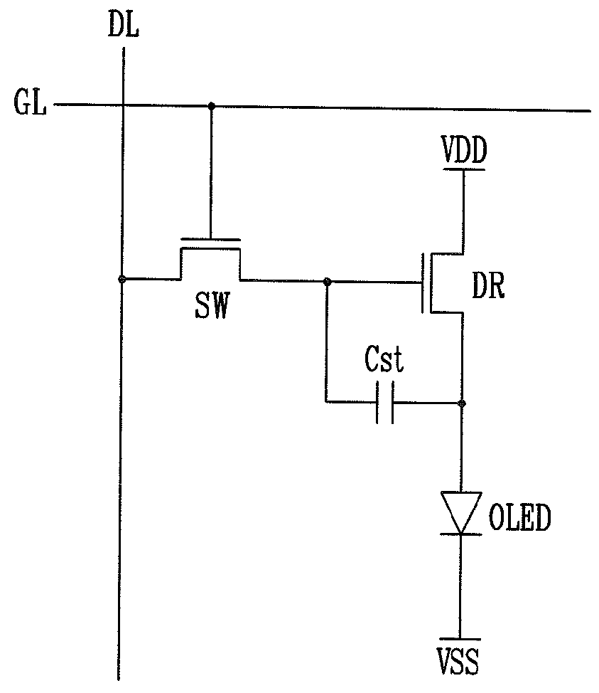
[0061]Here, a method for fabricating an OLED with respect to a pixel including 2T1C (two transistors and one capacitor) is taken as an example for the description purpose, but the present invention is not limited thereto.

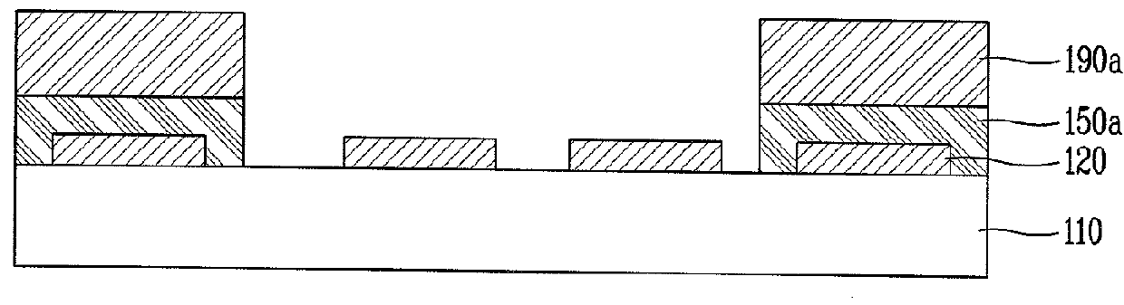
[0062]First, although not shown, in an OLED display device according to a first embodiment of the present invention, a gate line including a first gate electrode and a storage electrode including a second gate electrode may be formed on a substrate 110 made of an insulating material such as transparent glass, plastic, or the like.

[0063]A gate insulating layer made of silicon nitride (SiNx), silicon oxide (SiO2), or the like, may be formed on the gate line including the first gate electrode and the storage electrode in...

second embodiment

[0099]FIGS. 4A through 4H are sequential sectional views illustrating a method for fabricating an OLED display device according to the present invention, in which a method for fabricating an OLED diode with respect to some pixels is taken as an example.

[0100]Although not shown, as mentioned above, in an OLED display device according to a second embodiment of the present invention, a gate line including a first gate electrode and a storage electrode including a second gate electrode may be formed on a substrate 210 made of an insulating material such as transparent glass, plastic, or the like.

[0101]A gate insulating layer made of silicon nitride (SiNx), silicon oxide (SiO2), or the like, may be formed on the gate line including the first gate electrode and the storage electrode including the second electrode.

[0102]A first active layer and a second active layer, made of semiconductor, may be formed on the gate insulating layer. The first active layer and the second active layer may be...

third embodiment

[0128]FIGS. 5A through 5G are sequential sectional views illustrating a method for fabricating an OLED display device according to the present invention, in which a method for fabricating an OLED diode with respect to some pixels is taken as an example.

[0129]Although not shown, as mentioned above, in an OLED display device according to a third embodiment of the present invention, a gate line including a first gate electrode and a storage electrode including a second gate electrode may be formed on a substrate 310 made of an insulating material such as transparent glass, plastic, or the like.

[0130]A gate insulating layer made of silicon nitride (SiNx), silicon oxide (SiO2), or the like, may be formed on the gate line including the first gate electrode and the storage electrode including the second electrode.

[0131]A first active layer and a second active layer, made of semiconductor, may be formed on the gate insulating layer. The first active layer and the second active layer may be ...


PUM


Abstract

In an organic light emitting diode (OLED) display device and a method for fabricating the same, OLED pixels are patterned through a photolithography process, so a large area patterning can be performed and a fine pitch can be obtained, and an organic compound layer can be protected by forming a buffer layer of a metal oxide on an upper portion of the organic compound layer or patterning the organic compound layer by using a cathode as a mask, improving device efficiency. In addition, among red, green, and blue pixels, two pixels are patterned through a lift-off process and the other remaining one is deposited to be formed without patterning, the process can be simplified and efficiency can be increased.

Description

[0001]The present disclosure relates to subject matter contained in priority Korean Applications No. 10-2011-0095959, filed on Sep. 22, 2011, and No. 10-2012-0101196, filed on Sep. 12, 2012, which are herein expressly incorporated by reference in its entirety.1. FIELD OF THE INVENTION[0002]The present invention relates to organic light emitting diode (OLED) display device and a method of fabricating the same and, more particularly, to an OLED display device in which OLED pixels are patterned through a photolithography process, and a method of fabricating the same.2. DESCRIPTION OF THE RELATED ART[0003]Recently, as interest in information displays has been on the rise and demand for the use of portable information media has been increased, lightweight flat panel displays (FPDs) substituting cathode ray tubes (CRTs) as existing display devices have been actively researched and commercialized.[0004]In the FPD fields, a liquid crystal display (LCD) device, which is lighter and consumes ...

Claims


Application Information

Patent Timeline
Patent Type & Authority Applications(United States)
IPC IPC(8): H01L51/50H01L51/56
CPCH01L51/0016H01L51/0018H01L27/3218H01L27/3211H01L51/5234H10K59/35H10K59/353H10K71/221H10K71/233H10K50/828H01L27/153H01L33/62H01L33/20H10K50/11H10K50/15H10K50/16H10K50/17H10K50/171H10K71/00H10K71/10
Inventor KIM, YOUNG-MIYOON, JONG-GEUNHEO, JOON-YOUNGPARK, HAN-SUNDO, EUI-DOOLEE, YEON-KYEONG
Owner LG DISPLAY CO LTD
Why Eureka
Try Eureka