Connection structure of rigid printed circuit board and flexible circuit, the connection process and the circuit module using it

a technology of flexible circuits and printed circuit boards, which is applied in the direction of fixed connections, printed circuit components, printed circuit manufacturing, etc., can solve the problems of inability to obtain sufficient connection strength to withstand thermal stress or mechanical stress, increase costs, and risk of short circuits, and achieve low cost and high reliability

Inactive Publication Date: 2005-08-11
OPNEXT JAPAN INC
View PDF2 Cites 18 Cited by
  • Summary
  • Abstract
  • Description
  • Claims
  • Application Information

AI Technical Summary

Benefits of technology

[0009] In recent years, a demand is made that an optical module is downsized, high in reliability and low in the costs concurrently. In order to meet the demand, it is essential to make mass production with a connection structure using a flexible circuit of a high-precision fine pitch, and a facile connection process.

Problems solved by technology

However, in the case where the thickness of the solder plating is too thin, most of the solder 5 is extruded onto the wiring pattern 3 of the rigid printed circuit board 1 due to the thermo compression from above by the heating and pressurization tool 7, thereby making impossible to obtain a sufficient connection strength to withstand a thermal stress or a mechanical stress.
In addition, in the case where the solder is too thick, not only the sufficient connection strength cannot be obtained, but also the solder 5 is extruded between the adjacent conductive patterns 3 of the rigid printed circuit board 1 with the result that short-circuiting is liable to occur.
Therefore, the thickness of the solder plating is exact, thereby causing the costs to increase.
As a result, there is a risk that short-circuiting occurs between the adjacent conductive patterns, or gas remains in the solder as voids, to thereby deteriorate the connection strength.

Method used


Image

  • Connection structure of rigid printed circuit board and flexible circuit, the connection process and the circuit module using it
  • Connection structure of rigid printed circuit board and flexible circuit, the connection process and the circuit module using it
  • Connection structure of rigid printed circuit board and flexible circuit, the connection process and the circuit module using it

Examples


first embodiment

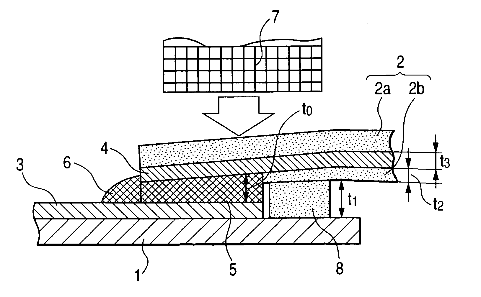
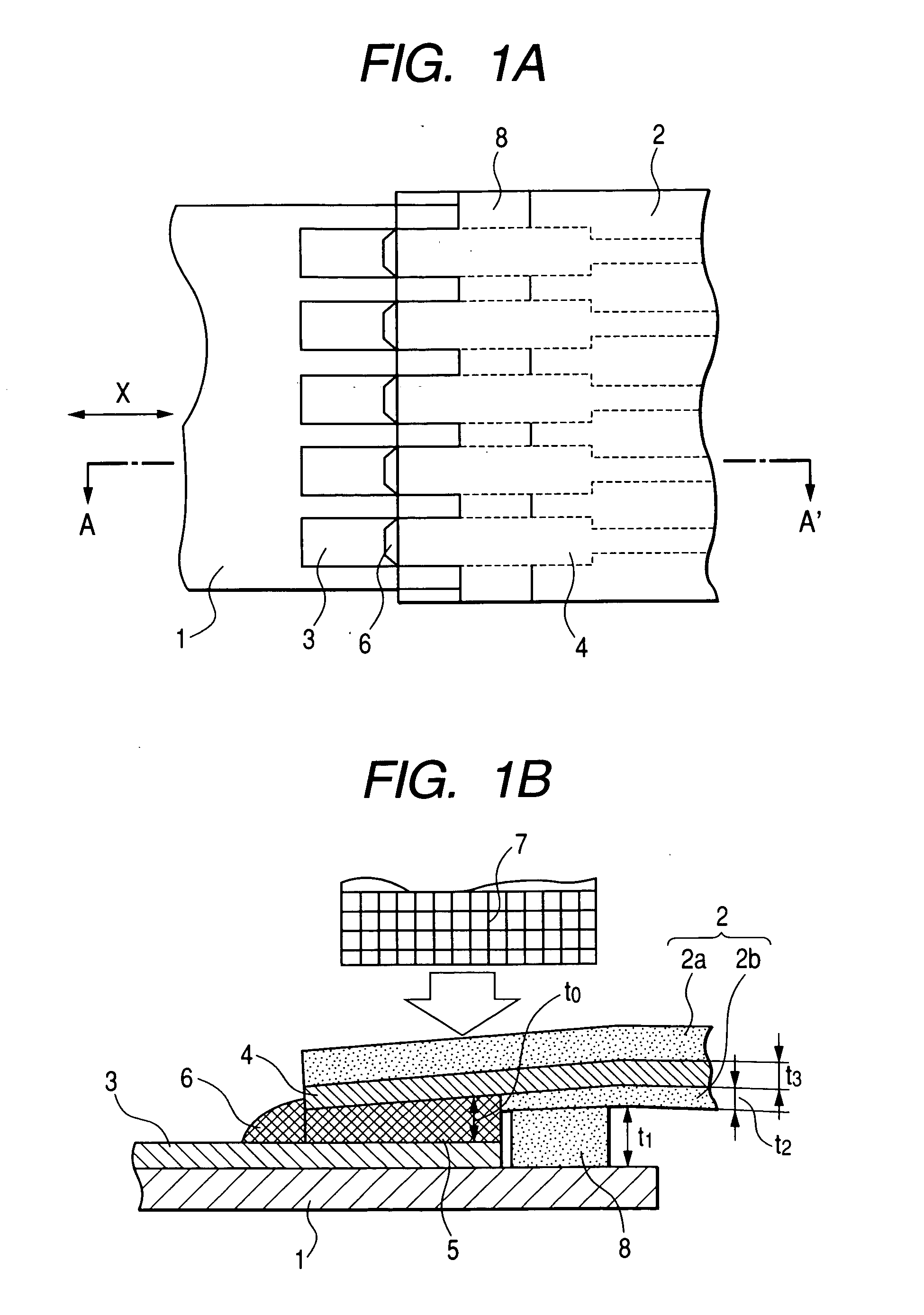
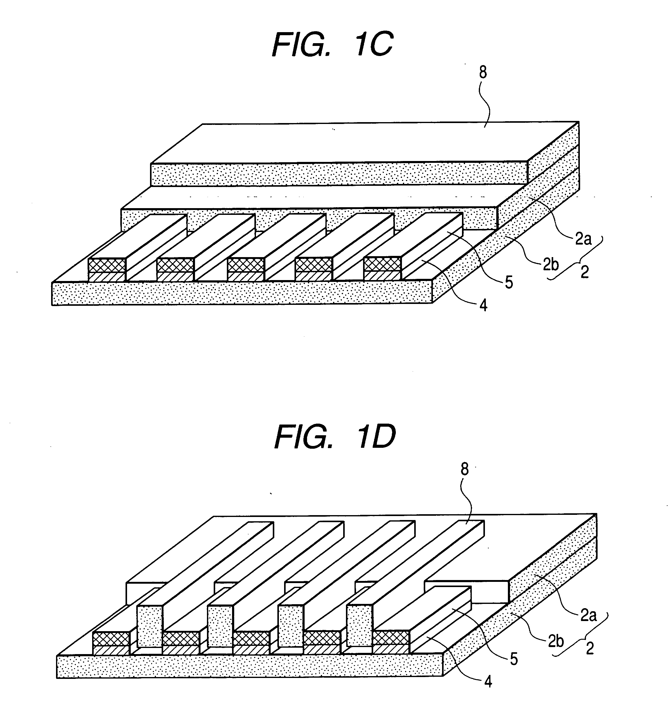
[0066]FIG. 1A is a plan view showing an example of a connection structure in which connection terminals 4 of a flexible circuit 2 are connected to connection terminals 3 of a rigid printed circuit board 1 with solder layers 5 according to the present invention. FIG. 1B is a cross-sectional view showing a connection process.

[0067] In the figures, reference numeral 1 denotes a rigid printed circuit board that is 0.5 to 2 mm in thickness, and 3 is a plurality of connection terminals (electrodes) corresponding to first connection terminals of the present invention, which are disposed on predetermined portions of the rigid printed circuit board at substantially regular intervals with widths of about 0.2 to 1 mm, lengths of 1.5 to 2 mm and pitches of 0.5 to 1 mm.

[0068] In the figures, reference numeral 2 denotes a flexible circuit that puts a conductive pattern by flexible insulating resin that is 20 to 60 μm in thickness. Reference numeral 4 denotes ends of the conductive pattern corre...

second embodiment

[0085] The connection structure of the solder connection portion between the rigid printed circuit board and the flexible circuit, and the connection process thereof according to another embodiment of the present invention will be described with reference to FIGS. 2A to 2C. FIG. 2A shows a plan view, and FIG. 2A shows a cross-sectional view taking along a line B-B′ of FIG. 2A. Fig. 2C shows a perspective view of the flexible circuit 2.

[0086] First, the connection process and the connection structure will be described with reference to FIGS. 2A and 2B. In the figures, reference numeral 1 denotes a rigid printed circuit board, 2 is a flexible circuit, 3 is connection terminals of the rigid printed circuit board which is about 0.3 mm in width, and 4 is connection terminals of the flexible circuit, which is about 0.3 mm in width and made of rolled copper excellent in flexibility and electric conductivity. Reference numeral 5 denotes a solder resulting from melting and solidifying the s...

third embodiment

[0091]FIG. 6 shows a plan view of an optical module, and shows the structure of the optical module having a transmission speed of 10 Gbps using the connection structure of the flexible circuit and the connection process thereof according to the present invention as described in the first and second embodiments. The structure of the optical module according to this embodiment will be described roughly. A main portion of the optical module is made up of a printed circuit board 10 on which a laser diode module 11 is mounted, a photodiode 9 that is connected to an optical connector 12, and a flexible circuit 2 that is electrically connected between the connection terminals of the photodiode 9 and the printed circuit board 10. Those components are received in an aluminum case 13.

[0092] The relationships with symbols in the figure will be described in more detail. Reference numeral 2 denotes a flexible circuit, 9 is a PDM (photo diode module), 10 is a printed circuit board, 11 is an LDM ...


PUM


Abstract

In a connection structure of a rigid printed circuit board and a flexible circuit each having a plurality of connection terminals, there are provided a connection structure that can obtain a necessary connection strength and prevent short-circuiting between adjacent connection terminals, and a connection process thereof. A rigid printed circuit board having a plurality of connection terminals is superimposed on a flexible circuit that puts a conductive pattern having connection terminals having the same configuration as that of the connection terminals of the rigid printed circuit board at an end thereof by flexible insulating resin, and connected to the flexible circuit with a solder due to thermo compression. A solder resist is disposed on the flexible insulating resin on the flexible circuit, and the solder connection can be realized by using a solder plating formed on one or both electrodes of the rigid printed circuit board and the flexible circuit while an amount of occlusion gas is controlled.

Description

CLAIM OF PRIORITY [0001] The present application claims priority from Japanese application serial No. 2004-003746, filed on (Jan. 9, 2004), the content of which is hereby incorporated by reference into this application. BACKGROUND OF THE INVENTION AND RELATED ART STATEMENT [0002] 1. Field of the Invention [0003] The present invention relates to a connection structure of a rigid printed circuit board and a flexible circuit, a connection process, and a circuit module using it, and more particularly to a connection structure of a rigid printed circuit board and a flexible circuit, which is suitable for a connection structure of a rigid printed circuit board and a flexible circuit such as an optical module, a connection process, and a circuit module using it. [0004] 2. Description of the Related Art [0005]FIGS. 3A and 3B show a conventional connection structure in which a flexible circuit 2 that puts a conductive pattern by two flexible insulating resin sheets is connected to a rigid pr...

Claims


Application Information

Patent Timeline
Patent Type & Authority Applications(United States)
IPC IPC(8): H01R43/02H01R4/02H05K1/14H05K3/34H05K3/36
CPCH01R4/02H01R12/62H05K3/3452H05K2201/2036H05K3/363H05K2201/09781H05K2201/09909H05K3/3473
Inventor KATAOKA, KOUICHIOHNO, KATSUYAOKAYAMA, SHINICHIURA, NOBUYUKIGOTO, FUMITOSHIKAKAMI, YUTAKA
Owner OPNEXT JAPAN INC
Why Eureka
Try Eureka