CMOS imager array with recessed dielectric

a dielectric array and image sensor technology, applied in the field of cmos (complementary metal oxide semiconductor) image sensor array structure, can solve the problem that the wiring requirements of dense logic circuits are different from those of imagers

Active Publication Date: 2008-05-22
GLOBALFOUNDRIES US INC
View PDF13 Cites 170 Cited by
  • Summary
  • Abstract
  • Description
  • Claims
  • Application Information

AI Technical Summary

Benefits of technology

[0008]The present invention is directed to a CMOS image sensor having a pixel array sensor portion that is thinner in a pixel array region compared to more dense logic wiring regions of the sensor. This allows the logic circuits to have as many metal levels as necessary to provide a dense layout, while still allowing the imager array to have a thin dielectric stack.
[0012]The method of fabricating a CMOS image sensor having a film stack that is thinner in the pixel array region as compared to the dense wiring logic regions of the chip results in a pixel array exhibiting increased light sensitivity.
[0026]Advantageously, the image sensor array of pixels formed in accordance with the method of the invention easily lends itself to conventional wafer level packaging in both Schott package and Shellcase package configurations.

Problems solved by technology

However, the requirements for wiring of dense logic circuits is different from that of imagers.

Method used


Image

  • CMOS imager array with recessed dielectric
  • CMOS imager array with recessed dielectric
  • CMOS imager array with recessed dielectric

Examples


Embodiment Construction

[0035]In the following description, numerous specific details are set forth, such as particular structures, components, materials, dimensions, processing steps and techniques, in order to provide a thorough understanding of the present invention. However, it will be appreciated by one of ordinary skill in the art that the invention may be practiced without these specific details. In other instances, well-known structures or processing steps have not been described in detail in order to avoid obscuring the invention.

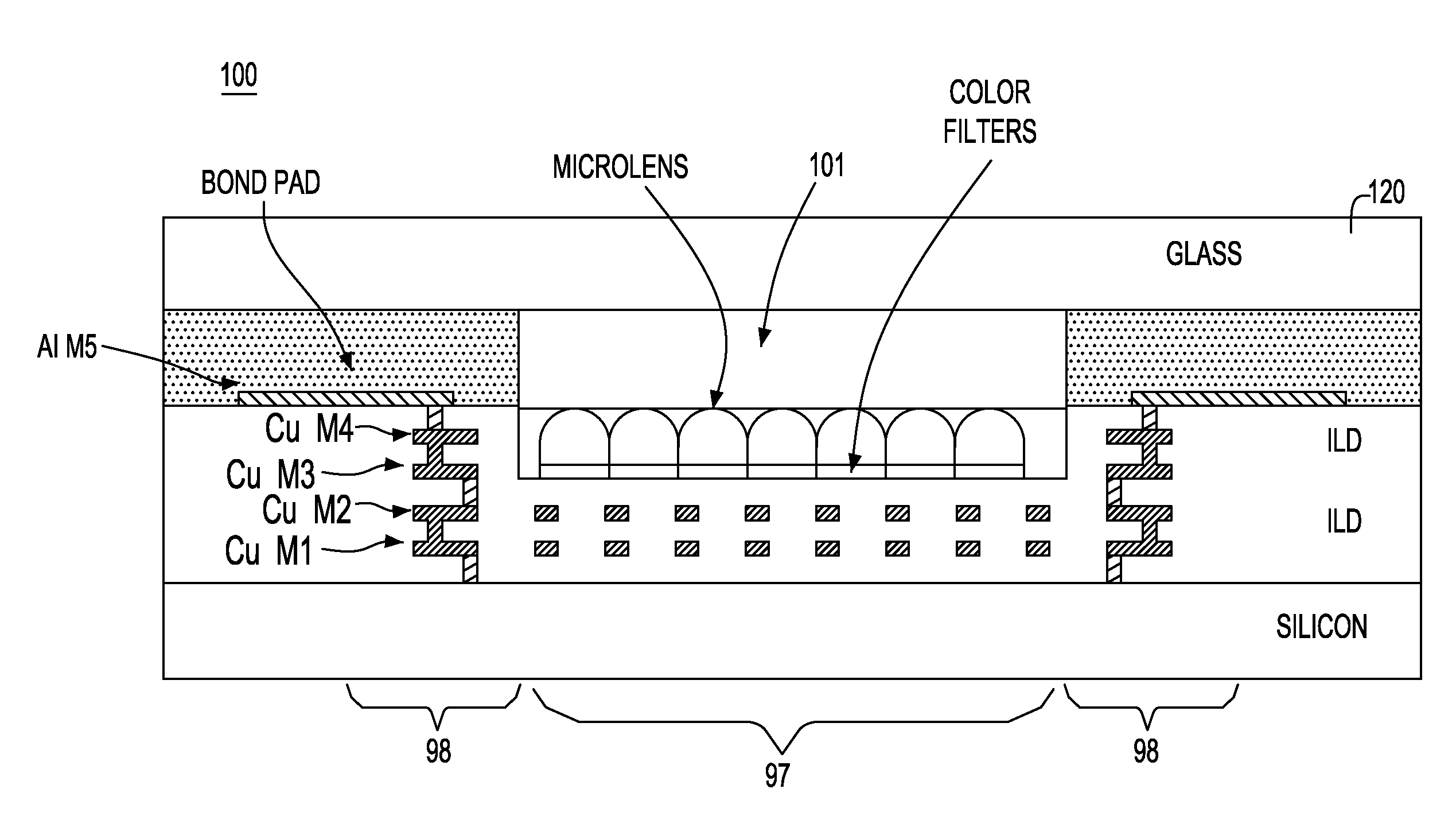
[0036]FIG. 3 illustrates, through a cross-sectional view, the CMOS image sensor chip 100 having a recessed dielectric according to a first embodiment of the invention. In this embodiment, the CMOS imager array 100 includes a recessed dielectric structure 101 in which is formed the array of color filters and corresponding microlens structures. The recess 101 particularly protects lenses during the process of bonding the glass plate 120 to the CMOS sensor array chip. Essent...


PUM


Abstract

A CMOS image sensor array and method of fabrication. The CMOS imager sensor array comprises a substrate; an array of light receiving pixel structures formed above the substrate, the array having formed therein “m” levels of conductive structures, each level formed in a corresponding interlevel dielectric material layer; a dense logic wiring region formed adjacent to the array of light receiving pixel structures having “n” levels of conductive structures, each level formed in a corresponding interlevel dielectric material layer, where n>m. A microlens array having microlenses and color filters formed above the interlevel dielectric material layer, a microlens and respective color filter in alignment with a respective light receiving structure formed at a surface of the substrate. A top surface of the interlevel dielectric material layer beneath the microlens array is recessed from a top surface of the interlevel dielectric material layers of the dense logic wiring region.

Description

FIELD OF THE INVENTION[0001]The present invention relates to semiconductor optical image sensors, and particularly, to a novel CMOS (complementary metal oxide semiconductor) image sensor array structure having a recessed dielectric thereby exhibiting reduced reflectivity and increased light sensitivity, and a process for manufacturing such image sensor array.DESCRIPTION OF THE PRIOR ART[0002]CMOS image sensors are beginning to replace conventional CCD sensors for applications requiring image pick-up such as digital cameras, cellular phones, PDA (personal digital assistant), personal computers, and the like, Advantageously, CMOS image sensors are fabricated by applying present CMOS fabricating process for semiconductor devices such as photodiodes or the like, at low costs. Furthermore, CMOS image sensors can be operated by a single power supply so that the power consumption for that can be restrained lower than that of CCD sensors, and further, CMOS logic circuits and like logic proc...

Claims


Application Information

Patent Timeline
Patent Type & Authority Applications(United States)
IPC IPC(8): H01L27/146H01L21/04
CPCH01L27/14618H01L27/14621H01L27/14687H01L27/14632H01L27/14685H01L27/14627H01L2224/02377H01L2224/05001H01L2224/05008H01L2224/05124H01L2224/05548H01L2224/05569H01L2224/05647H01L2224/13H01L2924/00014H01L27/146
Inventor ADKISSON, JAMES W.GAMBINO, JEFFREY P.HE, ZHONG-XIANGJAFFE, MARK D.LEIDY, ROBERT K.LUCE, STEPHEN E.RASSEL, RICHARD J.SPROGIS, EDMUND J.
Owner GLOBALFOUNDRIES US INC
Why Eureka
Try Eureka