BGA package with encapsulation on bottom of substrate

a technology of bga and substrate, applied in the field of bga (ball grid array) package with encapsulation on the bottom of the substrate, can solve problems such as product deficiencies, achieve the effects of reducing the exposed area of solder resist layer, improving the moisture resistance of semiconductor products of bga package, and preventing the falling of solder balls

Inactive Publication Date: 2008-05-22
POWERTECH TECHNOLOGY
View PDF5 Cites 27 Cited by
  • Summary
  • Abstract
  • Description
  • Claims
  • Application Information

AI Technical Summary

Benefits of technology

[0004]The primary object of the present invention is to provide a BGA package in order to solve the problems mentioned above, such as reducing exposed area of solder resist layer located on bottom of substra

Problems solved by technology

However, the BGA package cannot pass the MST level 1 (Moisture Sensitivity Test) all the time for which it is hard to deal moisture resistance since it has been developed, wherein MST is an international standard test such as published in JEDEC graded in 8 lev

Method used


Image

  • BGA package with encapsulation on bottom of substrate
  • BGA package with encapsulation on bottom of substrate
  • BGA package with encapsulation on bottom of substrate

Examples


first embodiment

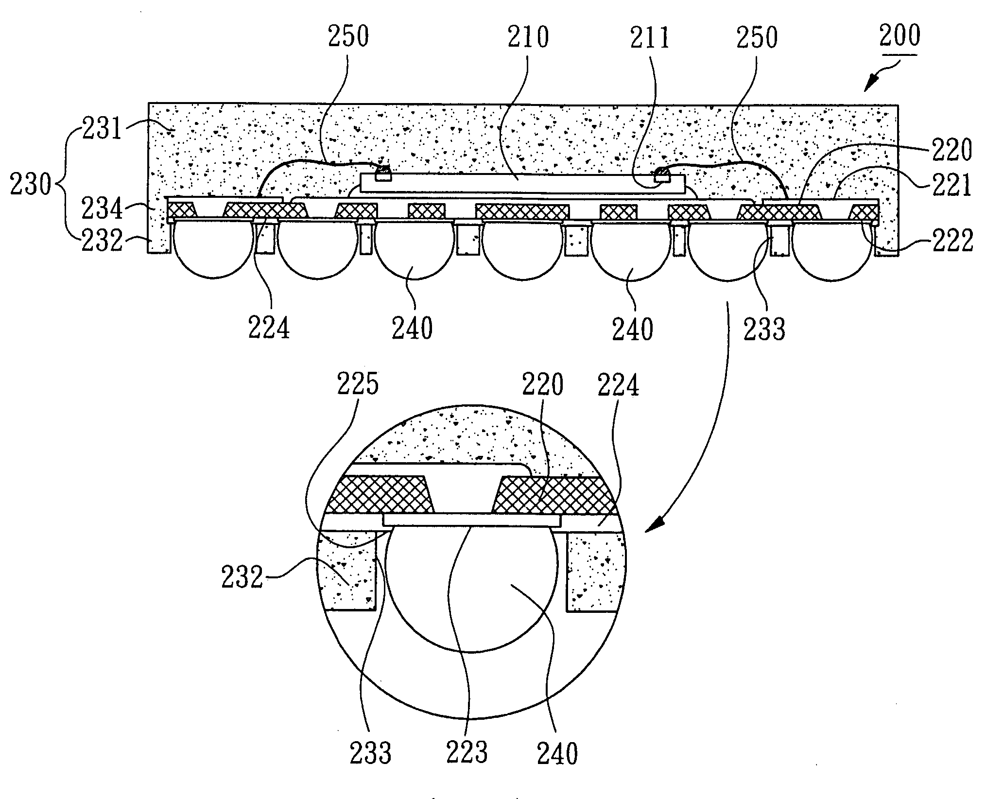
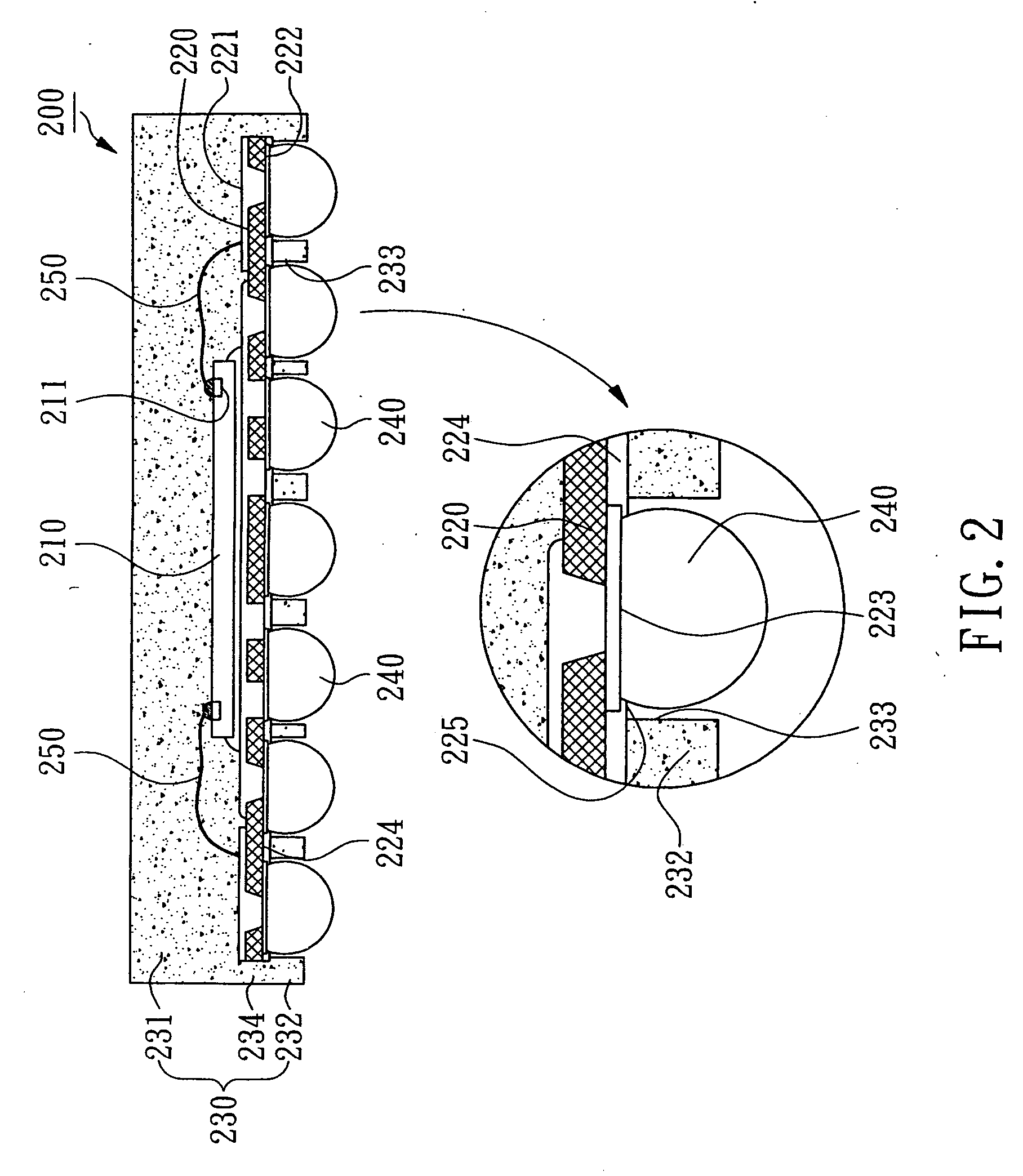
[0021]Referring to FIG. 2, therein is showed a BGA package in accordance with the present invention. The package 200 comprises a chip 210, a substrate 220, a molding compound 230 and a plurality of solder balls 240. The chip 210 made of semiconductor material may be an IC chip having a plurality of bonding pads 211 on the active surface thereof.

[0022]The substrate 220 that is utilized to carry the chip 210 and electrically connected to the chip 210 has an upper surface 221 and a lower surface 222, a plurality of ball pads 223 and a solder resist layer 224 are formed on the lower surface 222. The substrate 220 may be a multi-layer printed circuit board (PCB) including BT resin, for example. In this embodiment, the rear surface of the chip 210 is attached to the upper surface 221 of the substrate 220 by applying a chip-attaching material and the bonding pads 211 on the chip 210 are electrically connected to the substrate 220 via a plurality of bonding wires acting as electrical connec...

second embodiment

[0027]Furthermore, the present invention may be applied for various BGA package, such as the second embodiment showed in FIG. 3. A window type BGA package 300 comprises a chip 310, a printed circuit board 320, a molding compound 330 and a plurality of solder balls 340. A plurality of bonding pads 311 is formed on the active surface of the chip 310. The active surface of the chip 310 is attached to an upper surface 321 of the substrate 320. A lower surface 322 of the substrate 320 acting as a SMT surface on which the solder balls 340 are disposed. The substrate 320 further has a slot 326 and a plurality of electrical connection elements 350 such as bonding wires may pass through the slot 326 to electrically connect the bonding pads 311 of the chip 310 to the substrate 320. Besides, a plurality of ball pads 323 and a solder resist layer 324 are formed on the lower surface 322 of the substrate 320. The solder resist layer 324 has a plurality of openings 325 to expose at least a portion...

third embodiment

[0030]FIG. 4 shows a cavity-down BGA package 400 in the present invention, comprises a chip 410, a substrate 420, a molding compound 430, a plurality of solder balls 440 and further a thermal spreader 460 for disposing the substrate 420 and the chip 410. The chip 410 is disposed on the thermal spreader 460 through an opening of the substrate 420 that is meant the chip 410 is disposed inside the substrate 420. The substrate 420 has an upper surface 421 and a lower surface 422, and has a plurality of ball pads 423 and a solder resist layer 424 formed on the lower surface 422 of the substrate 420. Therein, the upper surface 421 is attached to the thermal spreader 460, A plurality of electrical connection elements 450 such as bonding wires are utilized to electrically connect the bonding pads 411 on the chip 410 to the substrate 420.

[0031]The molding compound 430 has a protrusion 432 as a main body to seal the chip 410 and the electrical connection elements 450. The molding compound 430...


PUM


Abstract

A BGA package with encapsulation on substrate bottom comprises a chip, a substrate, a molding compound and a plurality of solder balls. The substrate has a SMT surface placing a plurality of ball pads. The molding compound encapsulates a solder resist layer on the SMT surface of the substrate and has a plurality of through holes exposing the ball pads respectively. The hole diameter of the through holes is greater than that of the openings of the solder resist layer on the substrate to allow the solder balls not to contact the molding compound. The solder balls are disposed in the through holes and are bonded to the exposed ball pads of the substrate thereby enhancing moisture resistance of BGA products and preventing the solder balls from falling because of contact stress of the molding compound.

Description

FIELD OF THE INVENTION[0001]The present invention relates generally to a semiconductor package, and more specifically to a BGA (Ball Grid Array) package with encapsulation on bottom of substrate for enhancing product reliability by improving moisture resistance.BACKGROUND OF THE INVENTION[0002]A BGA package is one kind of semiconductor package design that has a plurality of solder balls arranged in array on bottom of a substrate for being surface mounted to an external PCB (Printed Circuit Board) thereby replacing conventional semiconductor package with leadframe acting as base, and slow transmissions because of overlong lead of leadframe won't happen. However, the BGA package cannot pass the MST level 1 (Moisture Sensitivity Test) all the time for which it is hard to deal moisture resistance since it has been developed, wherein MST is an international standard test such as published in JEDEC graded in 8 levels, level 1 has the most severe conditions.[0003]FIG. 1 shows a conventiona...

Claims


Application Information

Patent Timeline
IPC IPC(8): H01L23/48
CPCH01L23/3128H01L2224/32245H01L24/48H01L2224/16227H01L2224/48227H01L2224/4824H01L2224/73204H01L2224/73265H01L2924/15311H01L2924/15321H01L2924/18161H01L2224/16225H01L2224/32225H01L2224/48465H01L2224/73215H01L23/49816H01L2924/00H01L2924/00012H01L24/73H01L2924/00014H01L2224/45099H01L2224/45015H01L2924/207
Inventor FAN, WEN-JENG
Owner POWERTECH TECHNOLOGY
Why Eureka
Try Eureka