Spherical grid array encapsulation structure of base plate bottom glue encapsulation

An array packaging and structure technology, applied in the direction of semiconductor/solid-state device components, electrical components, electrical solid-state devices, etc., to achieve the effect of improving moisture resistance, reducing exposed area, and avoiding ball drop

Inactive Publication Date: 2008-01-16
POWERTECH TECHNOLOGY
View PDF0 Cites 6 Cited by
  • Summary
  • Abstract
  • Description
  • Claims
  • Application Information

AI Technical Summary

Problems solved by technology

[0007] Another object of the present invention is to provide a new type of ball grid array packaging structure. The technical problem to be solved is to make it possible to prevent the contamination of the molding compound at the bottom of the substrate by the opening size of the solder mask layer of the substrate. to the substrate ball pad, which is more suitable for practical

Method used


Image

  • Spherical grid array encapsulation structure of base plate bottom glue encapsulation
  • Spherical grid array encapsulation structure of base plate bottom glue encapsulation

Examples


Embodiment Construction

[0083] In order to further explain the technical means and effects of the present invention to achieve the intended purpose of the invention, the specific implementation of the ball grid array packaging structure proposed according to the present invention, with reference to the accompanying drawings and preferred embodiments, Structure, characteristic and effect thereof are as follows in detail.

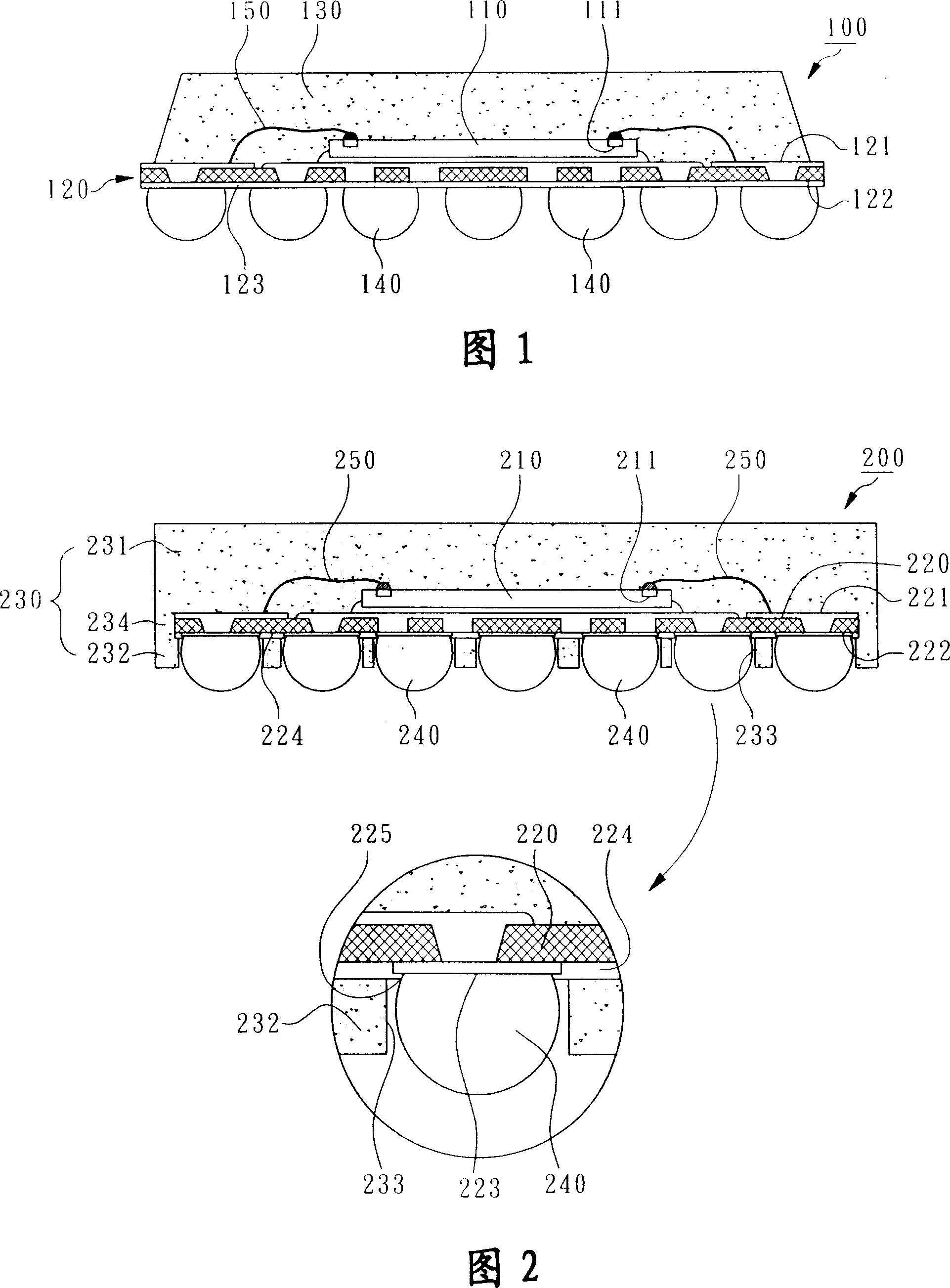
[0084] Please refer to FIG. 2 , which is a schematic cross-sectional view of a ball grid array package structure according to a first embodiment of the present invention. The BGA structure 200 mainly includes a chip 210 , a printed circuit board 220 , a molding compound 230 and a plurality of solder balls 240 .

[0085] The chip 210 is made of semiconductor material and can be an integrated circuit chip 210 with a plurality of welding pads 211 on its active surface.

[0086] The substrate 220 is used to carry the chip 210 and be electrically connected to the chip 210. The substrate...


PUM


Abstract

The invention relates to a ball grid array (BGA) encapsulating structure of adhesive-sealing the bottom of the baseplate, mainly comprising a wafer, a baseplate, a model encapsulating colloid and a plurality of solder balls. The baseplate has a surface jointing plate, and a plurality of ball pads and a solder-preventing layer. The model encapsulating colloid at least covers the surface jointing plate of the baseplate and has a plurality of ball-holding holes corresponding to the solder balls, and the sizes of the openings of the ball-holding holes are larger than those of the holes in the solder-preventing layer so as to keep the solder balls away from the model encapsulating colloid. The solder balls are aligned to the ball-holding holes and are jointed to the ball pads of the baseplate, by which the humidity resistance of BGA products is enhanced, and the solder balls are kept not to drop without the pushing from the stress of the encapsulating colloid.

Description

technical field [0001] The invention relates to a semiconductor packaging technology, in particular to a ball grid array packaging structure with glue on the bottom of the substrate, so as to improve product reliability of moisture resistance. Background technique [0002] The ball grid array package structure is provided with a plurality of matrix-arranged solder balls (solder balls) on the bottom of a substrate for surface bonding to an external printed circuit board, which can replace the traditional lead frame substrate semiconductor package structure, and does not There will be situations where the overly long pins of the lead frame affect the speed of electrical transmission. However, since the ball grid array packaging structure was developed, there has always been the problem of poor moisture resistance, usually failing to pass the first level of moisture sensitivity test (MST level 1), where MST is the abbreviation of Moisture Sensitivity Test, One can be found in ...

Claims


Application Information

Patent Timeline
Patent Type & Authority Applications(China)
IPC IPC(8): H01L23/498H01L23/31
CPCH01L2924/15311H01L2924/18161H01L2924/15322H01L2224/4824H01L2224/73204H01L2224/16225H01L2224/73265H01L2224/32245H01L2224/48227H01L2224/73215H01L2224/32225H01L24/73H01L2924/14
Inventor 范文正
Owner POWERTECH TECHNOLOGY
Why Eureka
Try Eureka