Memory module

Active Publication Date: 2008-05-29
MICRON TECH INC
View PDF6 Cites 23 Cited by
  • Summary
  • Abstract
  • Description
  • Claims
  • Application Information

AI Technical Summary

Benefits of technology

[0018]Another object of the present invention is to decrease the influence of a reflection of a signal from a terminal of a memory chip mounted on the back surface of a control chip.
[0020]According to the present invention, the first branch point is positioned at the control chip side. Therefore, the wiring length of the first wiring part can be made sufficiently short. Consequently, the period t1 shown in FIG. 7 can be substantially shortened, and the cross-point of the complementary signal can be made clear. Accordingly, the present invention can be remarkably suitable to the memory module that can perform a high-speed data transmission.

Problems solved by technology

As explained above, the conventional memory module has various problems regarding the wiring of the memory chips when the memory chips are mounted on the back surface of the memory buffer.

Method used


Image

  • Memory module
  • Memory module
  • Memory module

Examples


Embodiment Construction

[0032]Preferred embodiments of the present invention will be explained below with reference to the accompanying drawings.

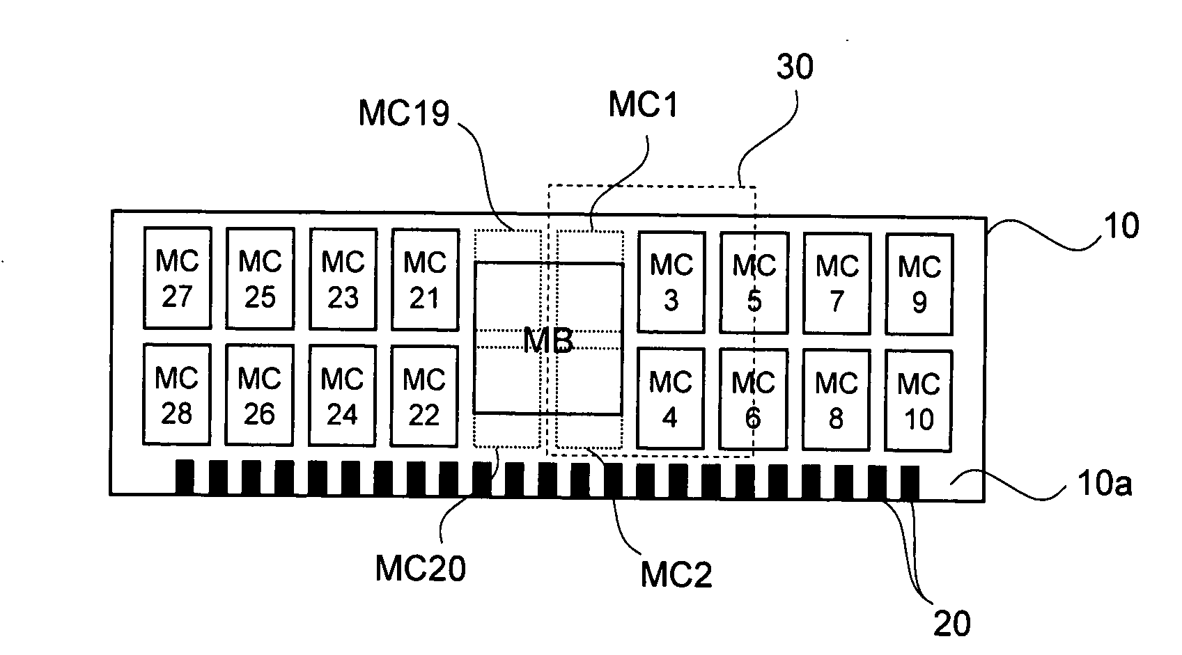
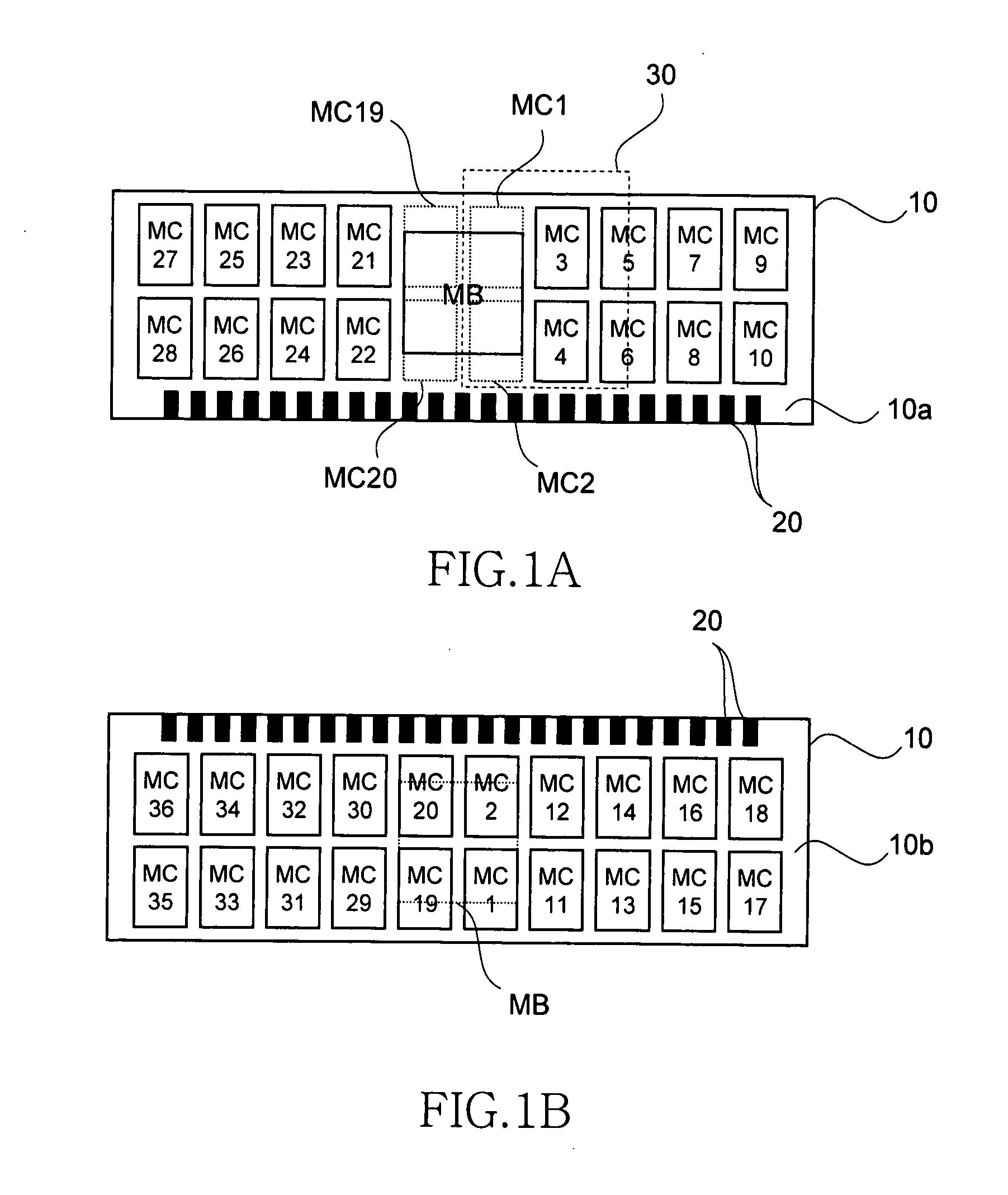
[0033]FIGS. 1A and 1B are schematic diagrams of a configuration of a memory module according to a preferred embodiment of the present invention. FIG. 1A is a top plan view of one surface of the memory module, and FIG. 1B is a top plan view of the other surface of the memory module.

[0034]As shown in FIGS. 1A and 1B, the memory module according to the present embodiment has a memory buffer MB and memory chips MC1 to MC36 mounted on a module substrate 10. The memory buffer MB is disposed at approximately the center of one surface 10a of the module substrate 10, and eight memory chips are disposed at each of both sides of the memory buffer MB. Therefore, 16 memory chips are disposed in total on the one surface 10a of the module substrate 10. Further, 20 memory chips are mounted on the other surface 10b of the module substrate 10. Accordingly, 36 memory chips are mount...


PUM


Abstract

A memory module includes a memory chip MC1 disposed at a position opposite to a memory buffer via a module substrate, a memory chip MC3 disposed at a position not opposite to the memory buffer via the module substrate, and a memory chip MC11 disposed at a position opposite to the memory chip MC3 via the module substrate. A branch point at which a wiring part connected to the memory chip MC1 and a wiring part connected to the memory chips MC3 and MC11 are branched is positioned at the memory buffer side from the viewpoint of the intermediate point between the planar mounting position of the memory buffer and the planar mounting position of the memory chips MC3 and MC11. Accordingly, the wiring length of the wiring part can be made sufficiently short.

Description

TECHNICAL FIELD[0001]The present invention relates to a memory module, and, more particularly to a memory module having a control chip such as a memory buffer and plural memory chips mounted on a module substrate, such as a DIMM (Dual Inline Memory Module)BACKGROUND OF THE INVENTION[0002]A DRAM (Dynamic Random Access Memory) is mainly used as a main memory in a personal computer or a server. It is common that the DRAM used for a main memory is mounted in advance on a memory module such as a DIMM, to facilitate operations of expansion.[0003]A memory module of a type called an Unbuffered memory module is widely used. However, the Unbuffered memory module employs a stab system for connecting all memory modules to the same channel. Therefore, when the number of memory modules is increased, the load on the channel increases accordingly. When the number of memory modules is increased, the number of branch points on the transmission line increases, and the signal quality is lowered.[0004]T...

Claims


Application Information

Patent Timeline
IPC IPC(8): H05K7/00
CPCG11C5/00H05K1/0298H05K1/181H05K2201/10545H05K2201/09627H05K2201/10159H05K2201/09254Y02P70/50
Inventor SUGANO, TOSHIOSAITO, SHUNICHIHIRAISHI, ATSUSHI
Owner MICRON TECH INC
Why Eureka
Try Eureka