
Printed circuit board assembly and display having the same

Inactive Publication Date: 2008-05-29
SAMSUNG ELECTRONICS CO LTD
View PDF56 Cites 12 Cited by
  • Summary
  • Abstract
  • Description
  • Claims
  • Application Information

AI Technical Summary

Benefits of technology

[0011]Exemplary embodiments of the present invention generally provide a printed circuit board (“PCB”) assembly capable of preventing a flex crack of a conductive pattern by increasing the area of the conductive pattern and covering the conductive pattern with a coverlay, and a display having the PCB assembly.
[0019]A chamfer or a curved surface may be provided on the coverlay to prevent the damage of the mounting unit when the cover layer contacts the mounting unit.

Problems solved by technology

Because the FPCB is shaped such that both ends are bent in directions opposite to each other, a bending force is distributed over the entire surface of the FPCB, which may cause a mounting of an electronic component to be damaged due to the bending force.
For example, the application of the bending force can result in cracking (also referred to as flex cracking) of a copper conductive pattern that is generally connected to the electronic component.
Once the crack is created, it may not be readily detected.
With time, temperature cycles and increased stress levels, the crack can grow.
The flex cracking of the copper conductive pattern, causes lower overall product yield and higher cost per good FPCB, since the cracked parts need to be discarded.

Method used


Image

  • Printed circuit board assembly and display having the same
  • Printed circuit board assembly and display having the same
  • Printed circuit board assembly and display having the same

Examples


Embodiment Construction

[0047]Hereinafter, exemplary embodiments of the present invention will be will be described in detail with reference to the accompanying drawings. In the drawings, the sizes and thicknesses of layers and regions may be exaggerated for clarity. Like reference numerals may refer to similar or identical elements throughout the description of the figures.

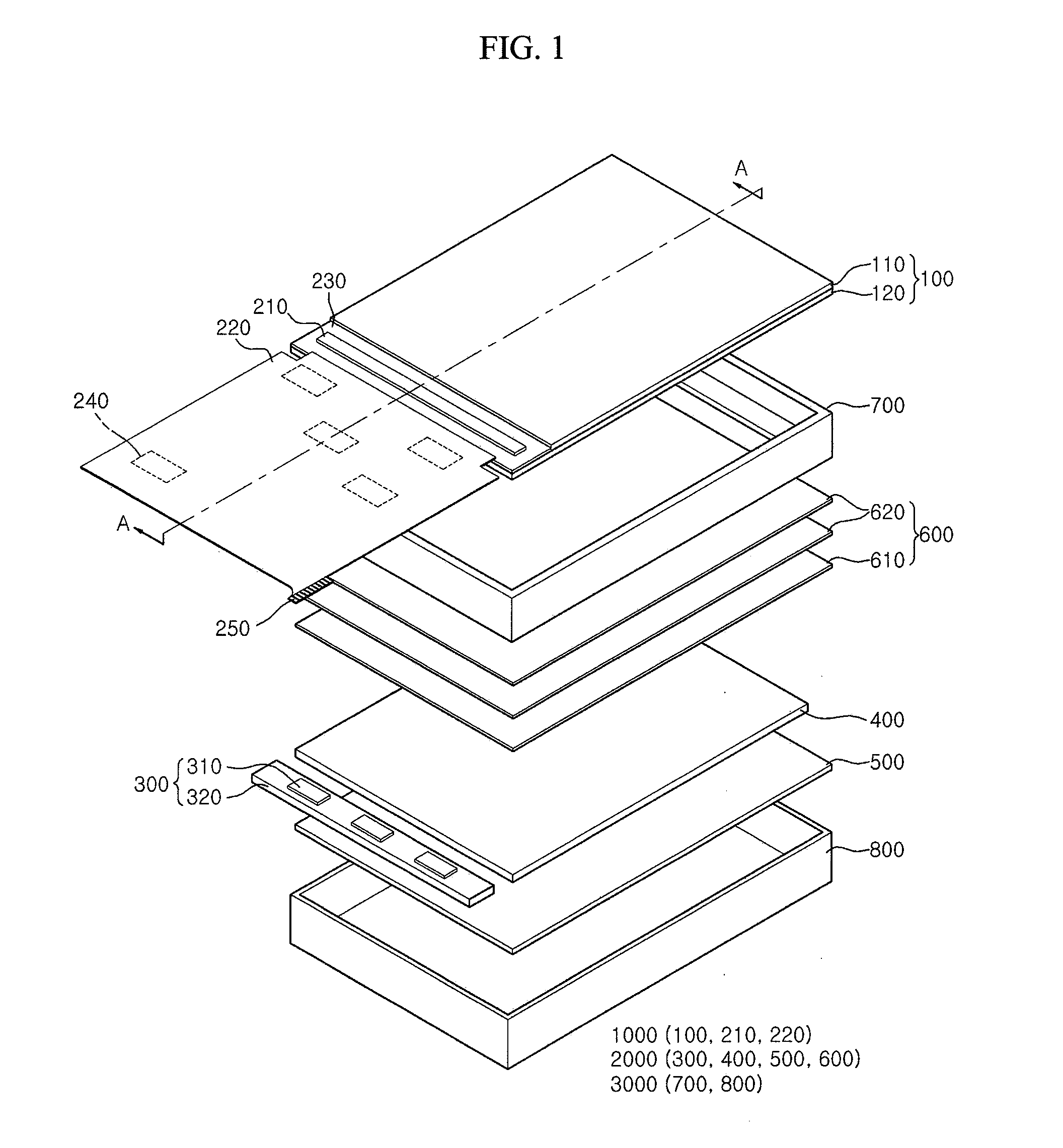
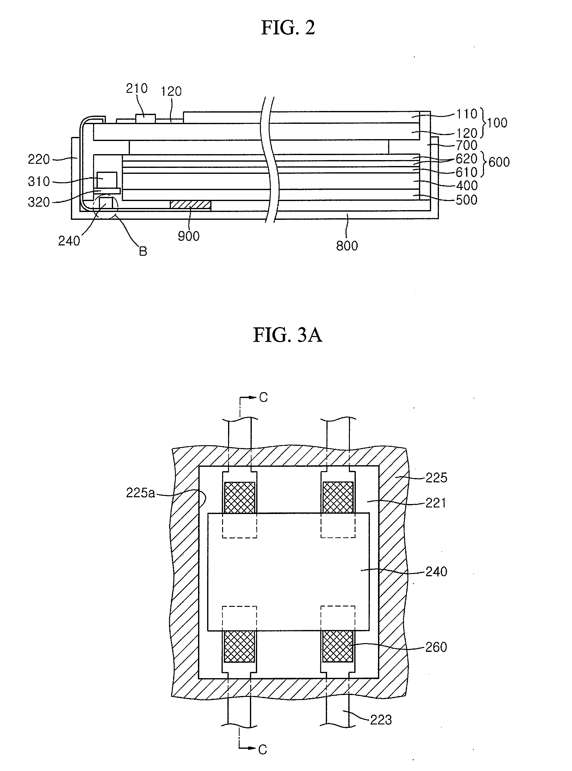
[0048]FIG. 1 is an exploded perspective view of an LCD in accordance with an exemplary embodiment of the present invention. FIG. 2 is a cross-sectional view taken along line A-A of FIG. 1.

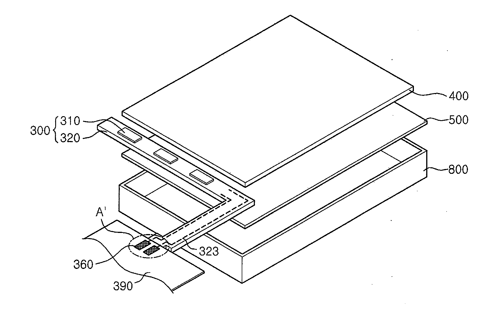
[0049]Referring to FIGS. 1 and 2, the exemplary LCD includes a display assembly 1000 (100, 210, 220), a backlight assembly 2000 (300, 400, 500, 600) configured to provide light to the display assembly 1000, a receiving member configured to receive and fix the display assembly 1000 and the backlight assembly 2000.

[0050]The display assembly 1000 includes an LCD panel 100, an integrated circuit (“IC”) chip 210 mounted at one side of the LCD panel 100, and...


PUM


Abstract

A PCB assembly includes a base, a conductive pattern disposed on the base, a pad provided on a portion of the conductive pattern, a mounting unit disposed on the pad for electrically connecting the conductive pattern and a coverlay having an opening that exposes the mounting unit

Description

CROSS-REFERENCE TO RELATED PATENT APPLICATIONS[0001]This application claims priority to Korean Patent Application Nos. 10-2006-110109, filed on Nov. 8, 2006, and 10-2007-109523 filed on Oct. 30, 2007, and all the benefits accruing therefrom under 35 U.S.C. §119, the contents of which are herein incorporated by reference in their entireties.BACKGROUND OF THE INVENTION[0002]1. Technical Field[0003]The present disclosure relates to electronic devices and, more particularly, to a printed circuit board (“PCB”) assembly and a display having the same.[0004]2. Discussion of Related Art[0005]A flat panel display is a type of display device that can be used to realize small-size, light-weight electronic devices such as a portable computer (e.g., a notebook computer), a personal digital assistant (PDA), and a mobile phone, as well as a monitor of a desktop computer. Examples of a flat panel display include a liquid crystal display (“LCD”), a plasma display panel (“PDP”) and a field emission di...

Claims


Application Information

Patent Timeline
IPC IPC(8): F21V23/00H05K7/02
CPCG02F1/13452H05K1/189H05K3/281H05K2203/0594H05K3/363H05K2201/099H05K2201/10727H05K3/3452
Inventor YOO, JONG KUNJOO, SOONG YONGLEE, JUNG SUNJUNG, SUK KILEE, DONG YUB
Owner SAMSUNG ELECTRONICS CO LTD
Learn More