Rectifier circuit, power supply circuit, and semiconductor device

a technology of rectifier circuit and power supply circuit, which is applied in the direction of electric variable regulation, process and machine control, instruments, etc., can solve the problems of deterioration or breakdown of semiconductor elements, withstand voltage gets low, and the voltage applied to transistors or diodes can be reduced, the effect of reducing the voltage applied to transistors or diodes

Inactive Publication Date: 2008-05-29
SEMICON ENERGY LAB CO LTD
View PDF6 Cites 260 Cited by
  • Summary
  • Abstract
  • Description
  • Claims
  • Application Information

AI Technical Summary

Benefits of technology

[0011]In addition, in order to reduce the cost of an integrated circuit, in general, the size of an integrated circuit formed of a semiconductor element is reduced by miniaturizing the semiconductor element and the number of integrated circuits that can be formed over one mother glass is increased. However, there is a problem that, when the semiconductor element is miniaturized, a withstand voltage gets low and thus an RF tag is more likely to be broken down due to excessive current.
[0028]Thus, even when noise which has a high frequency wave or a low frequency wave is included in a radio wave generated from the interrogator, the noise is unlikely to be included in a DC voltage generated in the power supply circuit. Consequently, operations of various circuits which operate using the DC voltage in the semiconductor device are unlikely to be affected by the noise; thus, operations of the semiconductor device can be stabilized.

Problems solved by technology

Therefore, there has been a problem in likeliness of deterioration or breakdown of the semiconductor element.
However, there is a problem that, when the semiconductor element is miniaturized, a withstand voltage gets low and thus an RF tag is more likely to be broken down due to excessive current.

Method used


Image

  • Rectifier circuit, power supply circuit, and semiconductor device
  • Rectifier circuit, power supply circuit, and semiconductor device
  • Rectifier circuit, power supply circuit, and semiconductor device

Examples


embodiment mode 1

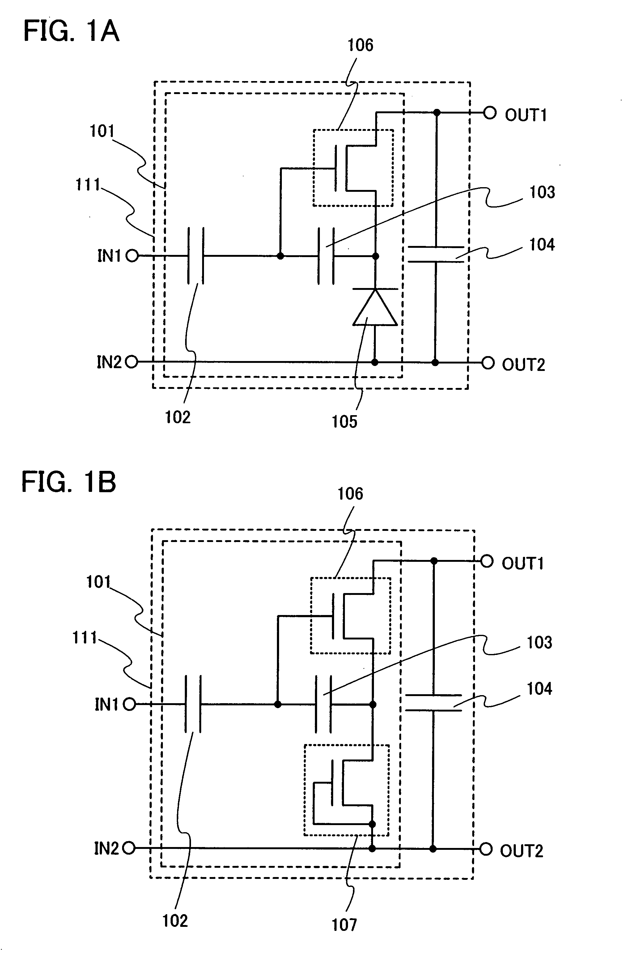
[0055]A structure of a rectifier circuit and a power supply circuit of the present invention will be described with reference to FIGS. 1A and 1B. In FIG. 1A, reference numeral 101 corresponds to a rectifier circuit of the present invention. The rectifier circuit 101 is connected to two input terminals IN1 and IN2 and two output terminals OUT1 and OUT2. Two terminals of an antenna are each connected to the input terminal IN1 or IN2. In addition, the rectifier circuit 101 has at least a first capacitor 102, a second capacitor 103, a diode 105, and a transistor 106. Note that FIG. 1A illustrates a structure of the rectifier circuit 101 in the case where the transistor 106 is an n-channel type. In addition, a power supply circuit 111 of the present invention has a third capacitor 104, in addition to the rectifier circuit 101.

[0056]The first capacitor 102, the second capacitor 103, and the diode 105 are sequentially connected in series in a path which connects the input terminal IN1 and ...

embodiment mode 2

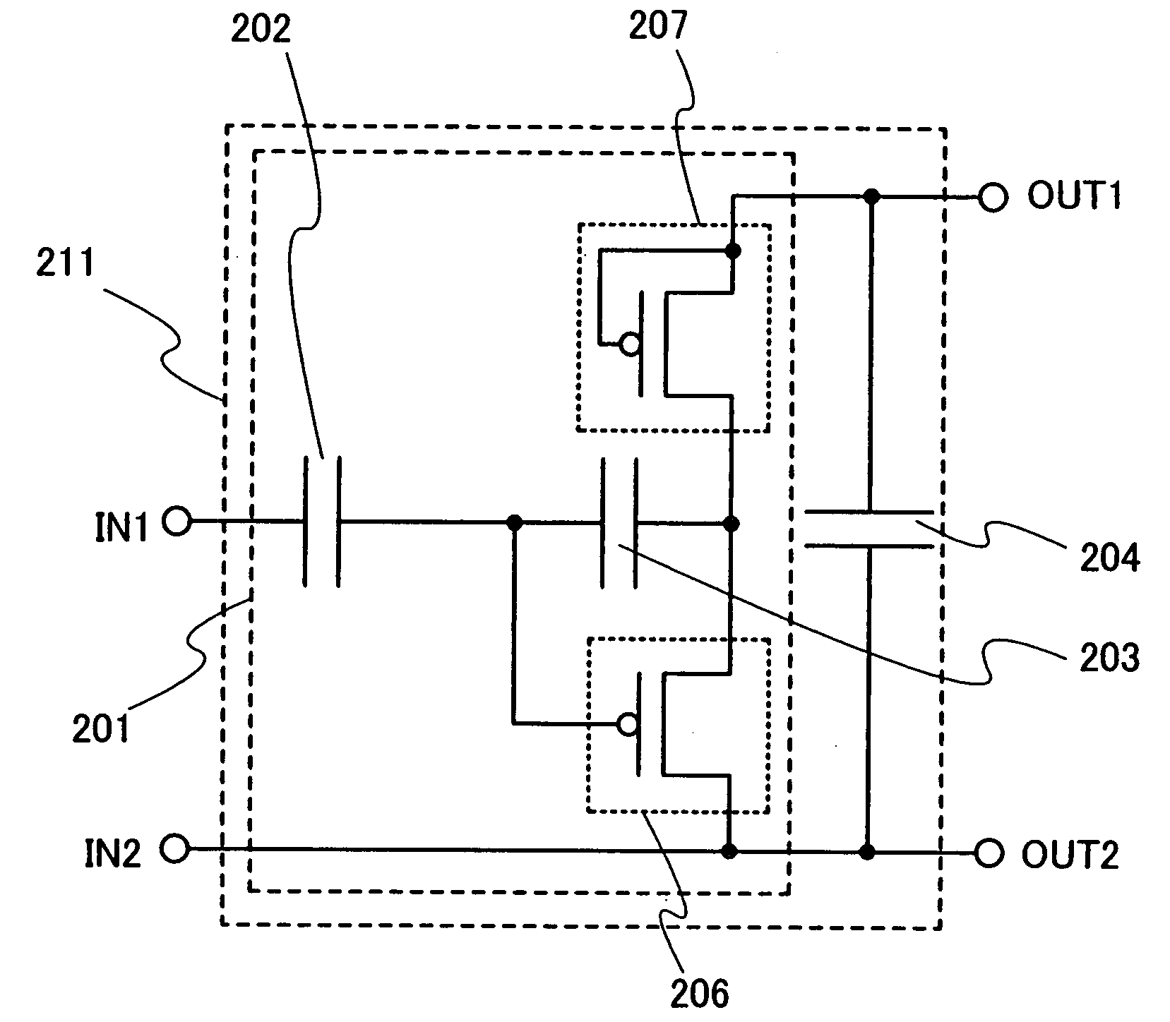
[0075]A structure of a rectifier circuit and a power supply circuit of the present invention will be described with reference to FIGS. 4A and 4B. In FIG. 4A, reference numeral 201 corresponds to a rectifier circuit of the present invention. The rectifier circuit 201 is connected to two input terminals IN1 and IN2 and two output terminals OUT1 and OUT2. Two terminals of an antenna are each connected to the input terminal IN1 or IN2. In addition, the rectifier circuit 201 has at least a first capacitor 202, a second capacitor 203, a diode 205, and a transistor 206. Note that FIG. 4A illustrates a structure of the rectifier circuit 201 in the case where the transistor 206 is a p-channel type. In addition, a power supply circuit 211 of the present invention has a third capacitor 204, in addition to the rectifier circuit 201.

[0076]The first capacitor 202, the second capacitor 203, and the diode 205 are sequentially connected in series in a path which connects the input terminal IN1 and t...

embodiment mode 3

[0095]In each of Embodiment Modes 1 and 2, the structure of the rectifier circuit and the power supply circuit which can obtain a positive DC voltage from the output terminal OUT1 is described. In this embodiment mode, a structure of a rectifier circuit and a power supply circuit of the present invention which can obtain a negative DC voltage will be described.

[0096]A structure of a rectifier circuit and a power supply circuit of this embodiment mode is illustrated in FIG. 7A. A rectifier circuit 301 illustrated in FIG. 7A is connected to two input terminals IN1 and IN2 and two output terminals OUT1 and OUT2. Two terminals of an antenna are each connected to the input terminal IN1 or IN2. In addition, the rectifier circuit 301 has at least a first capacitor 302, a second capacitor 303, a diode 305, and a transistor 306. Note that FIG. 7A illustrates a structure of the rectifier circuit 301 in the case where the transistor 306 is an n-channel type. In addition, a power supply circuit...


PUM


Abstract

It is an object of the present invention to provide a rectifier circuit that can suppress deterioration or dielectric breakdown of a semiconductor element due to excessive current. A rectifier circuit of the present invention includes at least a first capacitor, a second capacitor, and a diode which are sequentially connected in series in a path which connects an input terminal and one of two output terminals, and a transistor. The second capacitor is connected between one of a source region and a drain region and a gate electrode of the transistor. Further, the other one of the source region and the drain region and the other one of two output terminals are connected each other.

Description

BACKGROUND OF THE INVENTION[0001]1. Field of the Invention[0002]The present invention relates to a rectifier circuit which uses a diode and a power supply circuit which uses the rectifier circuit. More particularly, the present invention relates to a semiconductor device which uses the rectifier circuit or the power supply circuit and can perform wireless communication.[0003]2. Description of the Related Art[0004]Technology by which a signal is transmitted and received without contact between media (RF tags) each incorporating an integrated circuit and an antenna (RFID: Radio Frequency Identification) has been put to practical use in various fields and has been anticipated to further expand the market as a new mode of information communication. As the shape of an RF tag used for an RFID, a card shape or a chip shape which is smaller than such a card shape are employed in many cases; however, various shapes can be employed in accordance with an application.[0005]As for RFID, communic...

Claims


Application Information

Patent Timeline
Patent Type & Authority Applications(United States)
IPC IPC(8): H02M7/217H02J17/00H01L21/822H01L27/04H02M7/21
CPCH01L27/0629H01L27/13H01L27/12H01L27/0817
Inventor SHIONOIRI, YUTAKA
Owner SEMICON ENERGY LAB CO LTD
Why Eureka
Try Eureka