

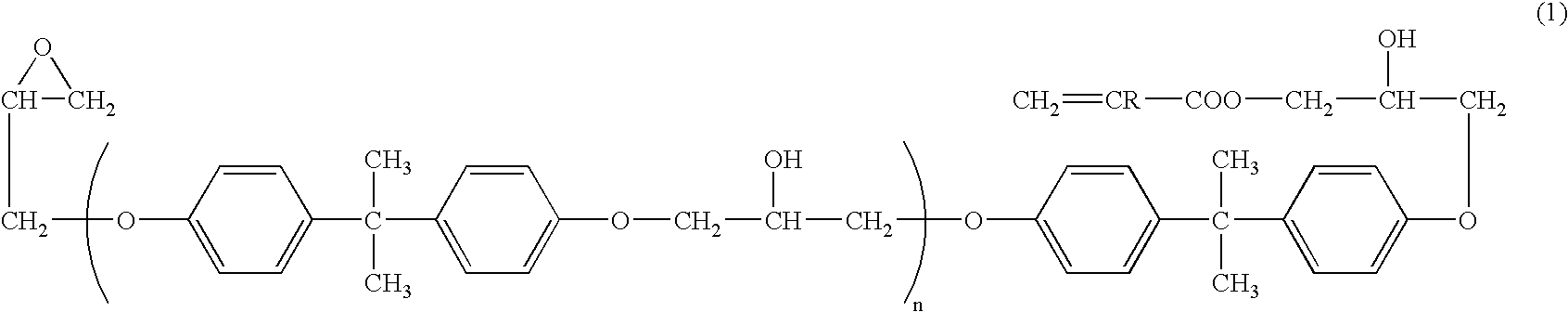
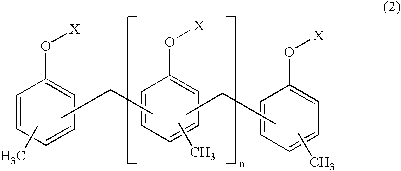
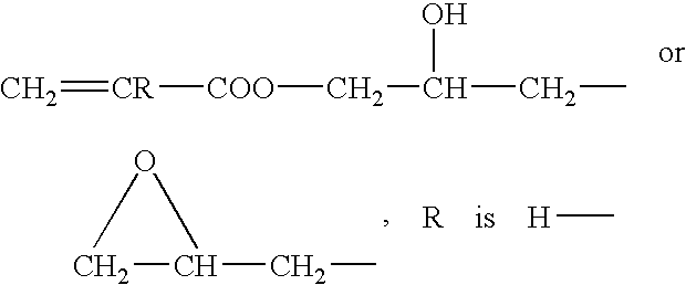
Adhesive Composition, Adhesive Sheet and Production Process for Semiconductor Device
a technology of adhesive sheet and semiconductor device, which is applied in the direction of solid-state devices, domestic applications, inks, etc., can solve the problems of reduced chip strength, severe physical properties of semiconductor devices, and reduced package reliability under severe hot and humid environment, so as to achieve high package reliability
- Summary
- Abstract
- Description
- Claims
- Application Information
AI Technical Summary
Benefits of technology
Problems solved by technology
Method used
Image

Examples
examples
[0101]Hereinbelow, the present invention shall be explained in detail with reference to examples, but the present invention shall not be restricted to these examples.
[0102]In the following examples and comparative examples, “evaluation of a surface mounting property” was carried out in the following manner.
Evaluation of Surface Mounting Property
(1) Production of Semiconductor Chip
[0103]Adhesive sheets prepared in the examples and the comparative examples were adhered on a ground surface of a #2000 ground silicon wafer (150 mm diameter and thickness 150 μm) by means of a tape mounter (Adwill RAD2500, manufactured by Lintec Corporation), and the wafer was fixed at a ring frame for wafer dicing. When the adhesive composition contained a photopolymerization initiator, the adhesive composition was then irradiated (350 mW / cm2, 190 mJ / cm2) with a UV ray from the base material side by means of a UV ray irradiating equipment (Adwill RAD2000, manufactured by Lintec Corporation).
[0104]Then, th...
PUM
| Property | Measurement | Unit |
|---|---|---|
| temperature | aaaaa | aaaaa |
| glass transition temperature | aaaaa | aaaaa |
| glass transition temperature | aaaaa | aaaaa |
Abstract
Description
Claims
Application Information