
Method of IC design optimization via creation of design-specific cells from post-layout patterns

a post-layout pattern and design optimization technology, applied in the field of process and system of integrated circuit (ic) design optimization, can solve the problems of inability to customize an ic, limited (static) set of standard cells in a library, labor-intensive custom design process, etc., and achieve the effect of improving a plurality of design objectives, nullifying inaccuracy of certain design metrics, and tight physical binding

Active Publication Date: 2008-05-29
ALPHAWAVE SEMI INC
View PDF3 Cites 171 Cited by
  • Summary
  • Abstract
  • Description
  • Claims
  • Application Information

AI Technical Summary

Benefits of technology

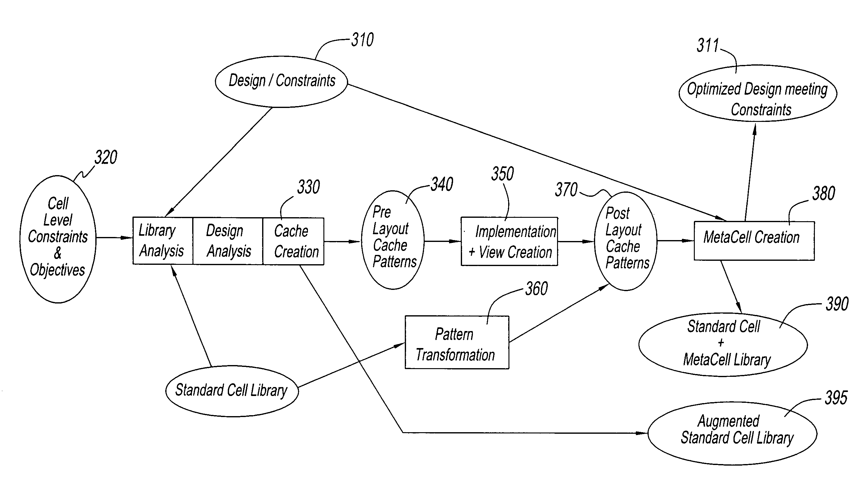
[0020]In one embodiment, an automatic scheme present in our disclosure can create arbitrarily complex metacells by transforming the underlying post-layout patterns.
[0021]In another embodiment, a manual scheme present in our disclosure can create arbitrarily complex metacells by transforming the underlying post-layout patterns. The manual scheme is guided by any end-user or entity to leverage any specific knowledge or limitation of the IC design flow.
[0026]The metacell (now indistinguishable from a standard cell) can be instantiated in the design to improve a plurality of design objectives such as, but not limited to, performance, area, power, noise, manufacturability, etc as well as a host of user-level customization directives such as, but not limited to, achieve tighter physical binding among a group of cells, nullify inaccuracy of certain design metrics and views, reuse certain functionality (as a standard cell) inter and intra-designs, etc.
[0027]Additional benefits of current disclosure include the following: analysis based cache generation framework can create an augmented standard cell library, having better quality of metric compared to input standard cell library. Augmented standard cell library can be used by any synthesis, physical synthesis or mapping technique to produce better quality of result for an IC design.

Problems solved by technology

For this reason, custom design process is labor-intensive, time consuming and expensive.
As such, resultant quality (area, speed, power, etc) of such designs is limited and inferior to that of custom-designed ICs.
In addition, the fixed (static) set of standard cells in a library is not amenable to the customization of an IC.
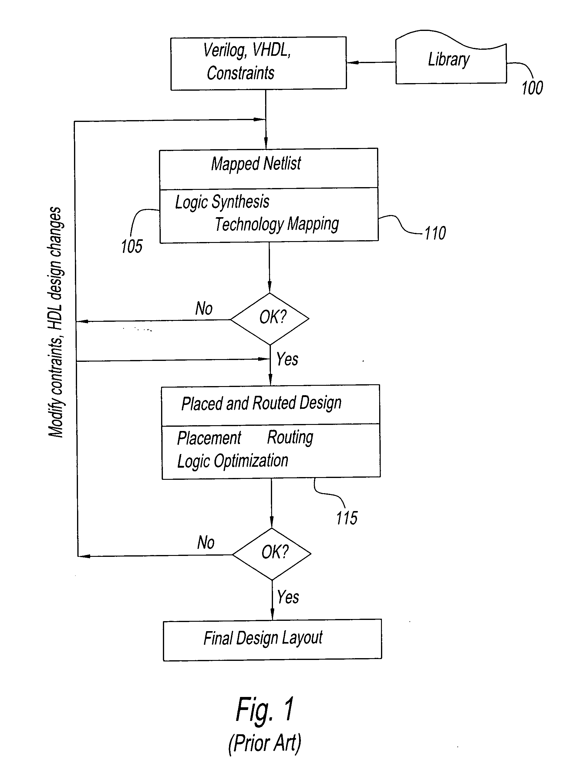
In the entire design process the contents of the library (100) remain unchanged, which often leads to designs with inferior quality and contribute to longer design cycle.
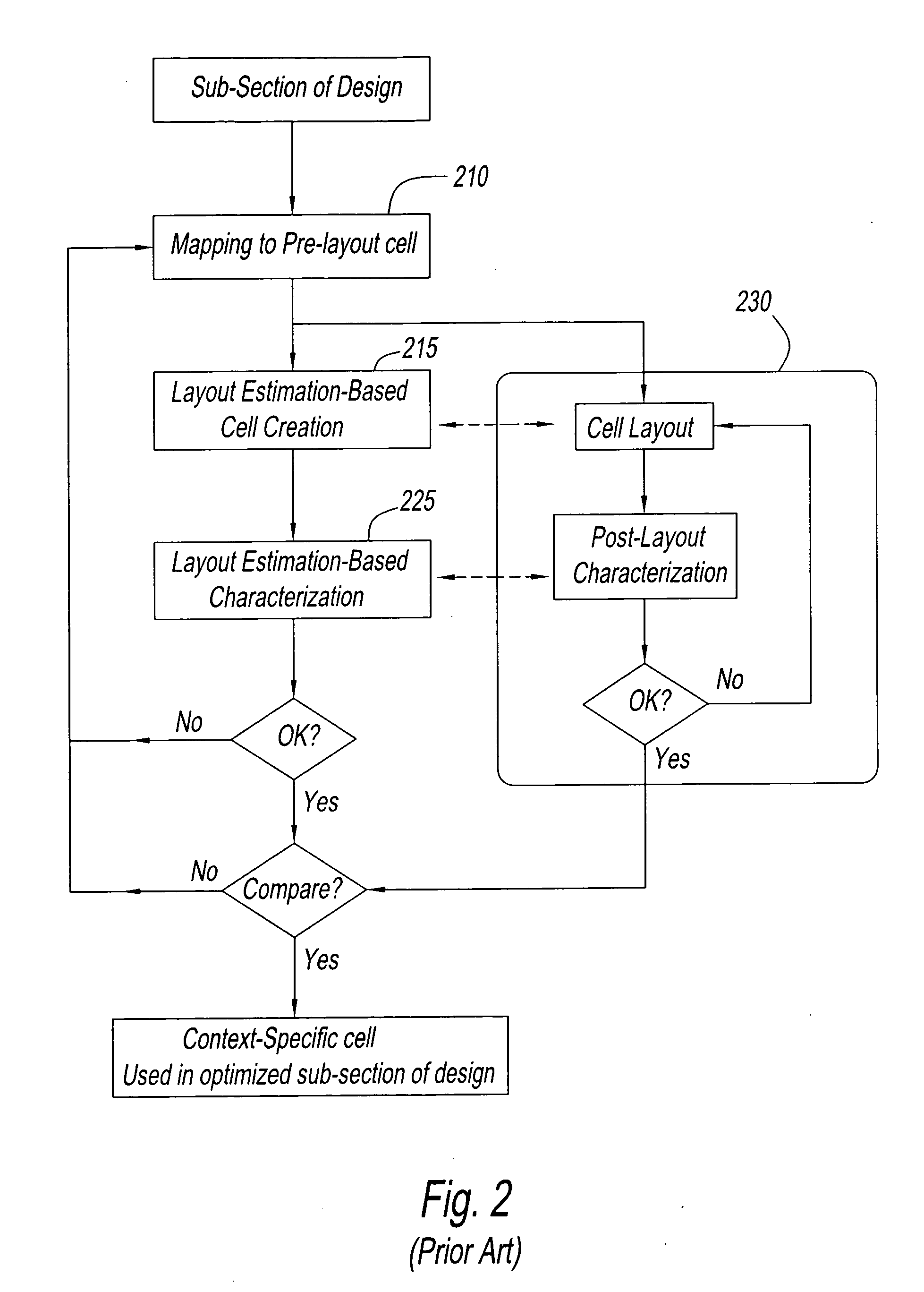
In deep sub-micron processes, these metrics, however, are often incapable of accurately predicting the layout characteristics that strongly determine the final quality (e.g., performance, area, power, noise, etc.) of the design-specific cell.
As a result, characterization (225) of the cell based on estimated layout parameters may be inaccurate.
In a nutshell, the limitation of this method lies in the fact that any decisions made prior to complete cell layout (230) may result in unnecessary transistor-level optimization iterations before the cell is accepted for use in the standard cell-based flow.
Cell layout synthesis (230) is a computationally intensive task and it may often be impractical to embed that process in the creation of on-the-fly design-specific standard cells.
On the other hand, without fully realizing and implementing the design-specific custom cells it is not possible to precisely converge on a design goal.
This difficulty coupled with the reliance on estimated layout characteristics results in an open-loop methodology (shown by dotted lines in FIG. 2) that is incapable of addressing the creation of design-specific standard cells in advanced deep sub-micron processes.

Method used


Image

  • Method of IC design optimization via creation of design-specific cells from post-layout patterns
  • Method of IC design optimization via creation of design-specific cells from post-layout patterns
  • Method of IC design optimization via creation of design-specific cells from post-layout patterns

Examples


Embodiment Construction

[0047]A method for optimizing an integrated circuit design comprising: creating a cache of post-layout patterns; and optimizing the integrated circuit design using the cache of post-layout patterns to create design-specific and / or context-specific standard cells. The cache of post-layout patterns is created by the method comprising: analyzing a standard cell library for the distribution of cell characteristics over the various cells in each logic family and / or analyzing the standard cell library to determine the layout architectures of the cells; optionally, enhancing the standard cell library by adding new cells, wherein the new cells are based on the results of the analysis of cell characteristics and layout architectures, thereby combining the new cells with the standard cell library to create an augmented cell library; creating standard cell fragments, where the standard cell fragments are integrated circuit layouts that can be combined to construct a new standard cell, in whole...


PUM


Abstract

A closed-loop IC design optimization process by automatically or manually creating design-specific cells with desired characteristics (e.g., performance, area, power, noise, etc.), which will be then implemented as a standard cell (also known hereafter as metacell), from a set of post-layout patterns. A post-layout pattern represents a part or whole of a standard cell and contains information regarding the pattern including, but not limited to, layout, timing, area, power and noise. As the metacells are created from post-layout patterns, the inaccuracies of prior dynamic library techniques are easily avoided. Such metacells, being design-specific, are optimized to satisfy the constraints imposed by the design context, thus bringing the powerful design-specific customization to standard cell-based design methodology.

Description

CROSS-REFERENCED APPLICATIONS[0001]This application claims priority to U.S. Provisional Patent Application No. 60 / 809,132, filed on May 26, 2006, which is incorporated herein in its entirety.BACKGROUND[0002]1. Field of the Disclosure[0003]The present disclosure relates generally to a process and system of integrated circuit (IC) design optimization by automatically or manually creating design-specific cells with desired characteristics (such as, but not limited to performance, area, power, noise, etc.) that are implemented as standard cells from a set of post-layout patterns. A post-layout pattern represents a part or whole of a standard cell and contains information regarding the pattern including, but not limited to, layout, timing, area, power and noise.[0004]2. Discussion of the Background Art[0005]Incessant progress in IC manufacturing technologies is enabling the design of ever larger and complex circuits. The process of designing ICs can be broadly classified into two categor...

Claims


Application Information

Patent Timeline
Patent Type & Authority Applications(United States)
IPC IPC(8): G06F17/50
CPCG06F17/505G06F30/327
Inventor MAJUMDER, PURNABHAKUMTHEKAR, BALAKRISHNASHAH, NIMISH RAMESHBHAIMOWCHENKO, JOHNCHAVDA, PRAMIT ANIKUMARKOJIMA, YOSHIHISAYOSHIDA, HIROAKIBOPPANA, VAMSI
Owner ALPHAWAVE SEMI INC
Learn More