Plasma display panel and field emission display

a display panel and display panel technology, applied in the field of plasma display panel and field emission display, can solve the problems of insufficient anti-reflection function, difficult to perform anti-reflection process with respect to all light incident from external from a variety of different angles, etc., and achieve the effect of improving image quality, improving performance, and improving anti-reflection performan

Inactive Publication Date: 2008-06-05
SEMICON ENERGY LAB CO LTD
View PDF53 Cites 23 Cited by
  • Summary
  • Abstract
  • Description
  • Claims
  • Application Information

AI Technical Summary

Benefits of technology

[0009]It is an object of the present invention to provide a PDP and an FED with excellent visibility that each have an antireflective function by which reflection of external light can be reduced.
[0027]In the present invention, a PDP and an FED that each have an antireflective layer that has a plurality of pyramidal projections over its surface and an even higher level antireflective function by which the reflection of incident light from external can be reduced by covering of the pyramidal projections with covering films, where each of the covering films has a higher index of refraction than that of the pyramidal projection, can be provided. Consequently, a PDP and an FED, each with even higher image quality and higher performance, can be manufactured.

Problems solved by technology

Furthermore, in order to make the light from external cancel itself out, there is a need to closely control the optical characteristics, film thicknesses, and the like of materials used for the films that are stacked together, and it is difficult to perform antireflective processes with respect to all light that is incident from external from a variety of different angles.
In addition, even with the conical or pyramidal antireflective structures, there has not been enough antireflective function.

Method used


Image

  • Plasma display panel and field emission display
  • Plasma display panel and field emission display
  • Plasma display panel and field emission display

Examples


embodiment mode 1

[0058]In the present embodiment mode, in a PDP and an FED of the present invention, an antireflective layer provided in a PDP or an FED will be described. Specifically, an example of an antireflective layer that has an antireflective function by which the reflection of light from external on a surface of the PDP or FED can be reduced and which is used to grant excellent visibility to a PDP or an FED.

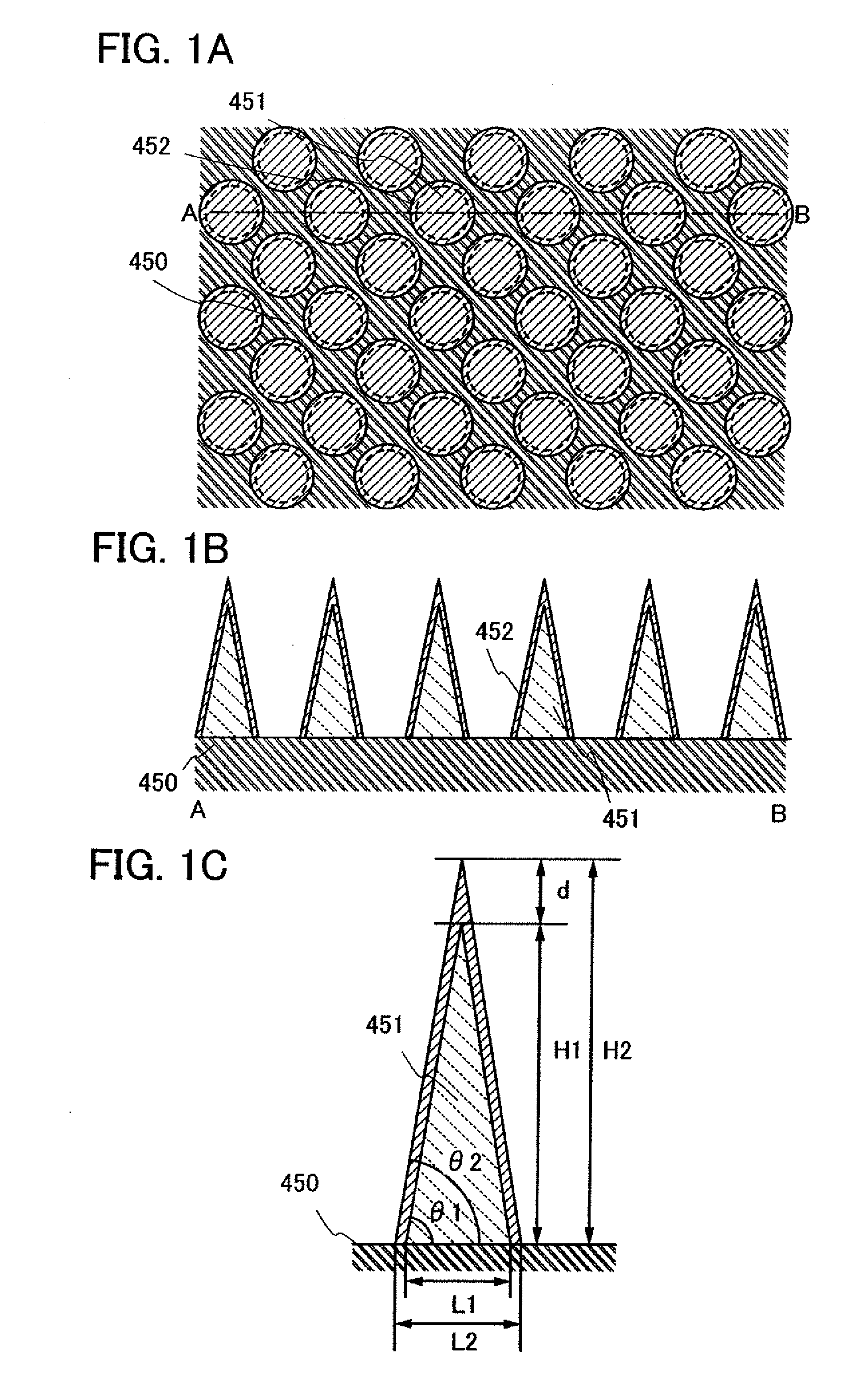
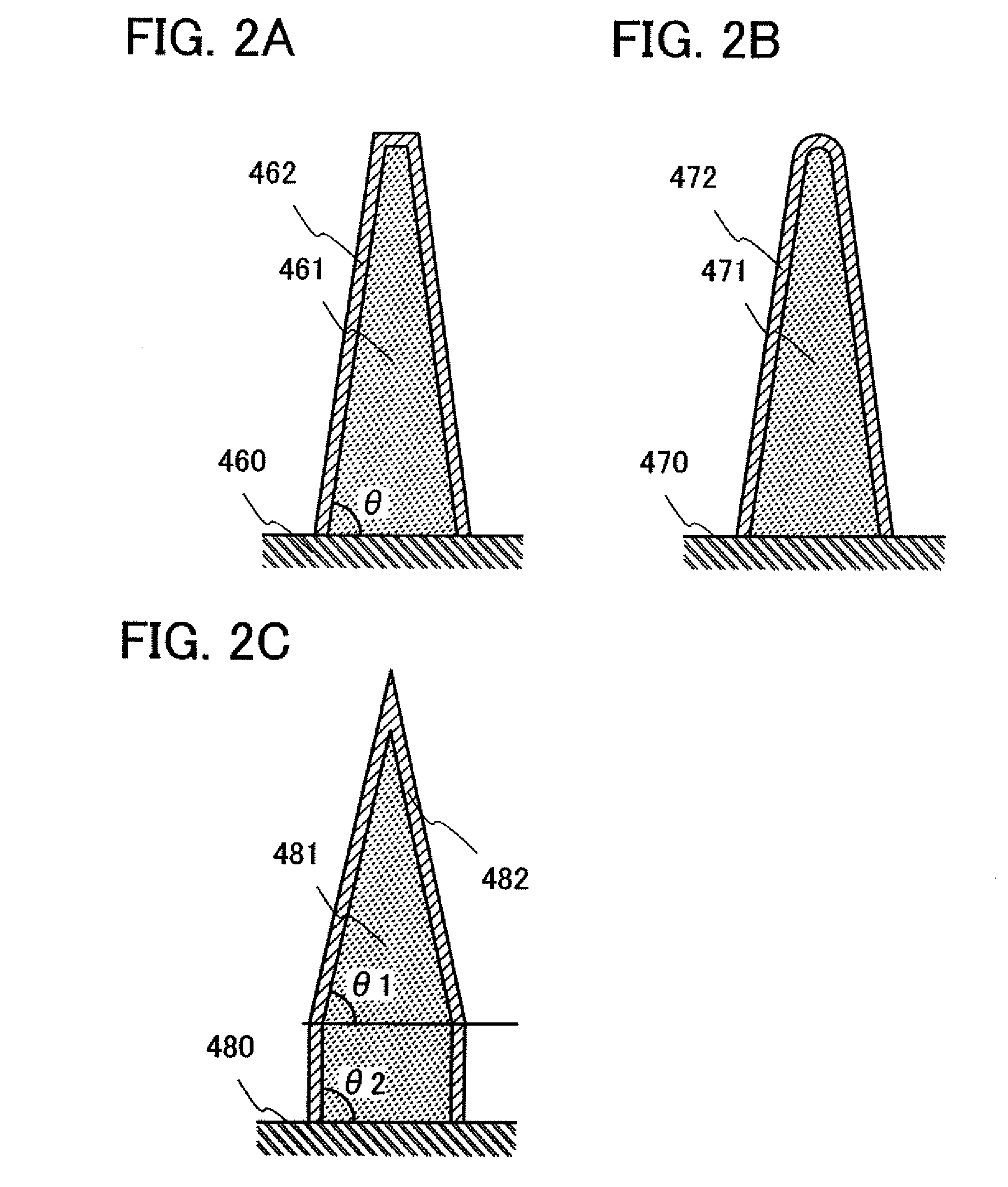
[0059]FIG. 1A is a top-view diagram and FIGS. 1B and 1C are cross-sectional view diagrams of an antireflective layer used in the present invention. In FIGS. 1A to 1C, a plurality of projections 451 and a covering film 452 are provided over a display screen 450. The antireflective layer is made up of the plurality of projections 451 and the covering film 452. FIG. 1A is a top-view diagram of a PDP or an FED of the present embodiment mode, and FIG. 1B is a diagram of a cross section taken along line A-B in FIG. 1A. FIG. 1C is an exploded-view diagram of FIG. 1B. As shown in FIGS. 1A and 1B...

embodiment mode 2

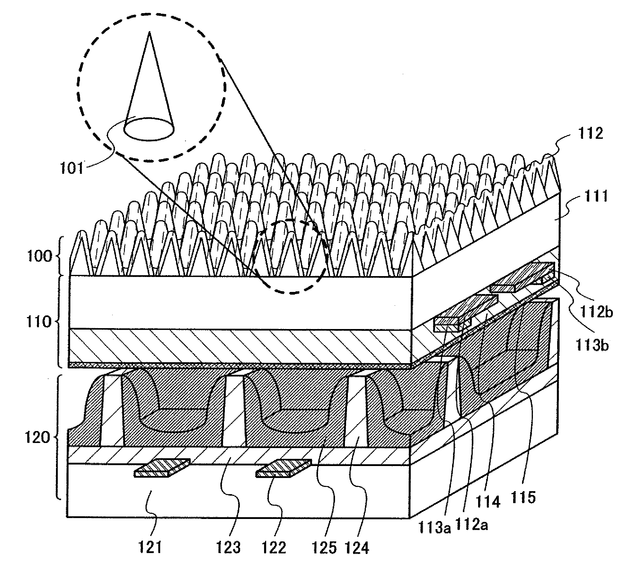
[0094]In the present embodiment mode, a PDP, the object of which is to have an antireflective function by which the reflection of incident light from external can be reduced even more and to provide a display device with excellent visibility, is described. That is, the details of a structure of a PDP that has a pair of substrates, at least one pair of electrodes provided between the pair of substrates, a phosphor layer provided between the pair of electrodes, and an antireflective layer provided on the outer side of one of the pair of substrates are given.

[0095]In the present embodiment mode, an alternating current discharge (AC type) surface emission PDP is given. As shown in FIG. 9, in the PDP, a front substrate 110 and a back substrate 120 are placed opposite from each other, and the periphery of the front substrate 110 and the back substrate 120 is sealed in with a sealant (which is not shown). Furthermore, areas between the front substrate 110, the back substrate 120, and the s...

embodiment mode 3

[0148]In the present embodiment mode, an FED, the object of which is to have an antireflective function by which the reflection of incident light from external can be reduced even more and to provide a display device with excellent visibility, is described. That is, the details of a structure of an FED that has a pair of substrates, an electron emitter provided in one of the pair of substrates; an electrode provided in the other one of the pair of substrates; a phosphor layer provided in contact with the electrode; and an antireflective layer provided in the outer side of the other one of the pair of substrates are given.

[0149]An FED is a display device in which a phosphor is excited by an electron beam and emits light. FEDs can be separated into diode-type, triode-type, and tetrode-type according to electrode classification.

[0150]In a diode-type FED, a rectangular cathode electrode is formed over a surface of a first substrate, a rectangular anode electrode is formed over a surface...


PUM

PropertyMeasurementUnit
heightaaaaaaaaaa
heightaaaaaaaaaa
widthaaaaaaaaaa

Abstract

It is an object of the present invention to provide a PDP and an FED with excellent visibility and a high level of reliability that each have an antireflective function by which reflection of external light can be reduced. A plurality of adjacent pyramidal-shaped projections and an antireflective layer equipped with a covering film that covers the projections are provided. The reflection of light is prevented by the index of refraction of incident light from external being changed by a pyramid, which is a physical shape, projecting out toward an external side (atmosphere side) of a substrate that is to be used as a display screen as well as by the covering film used to cover the projections being formed of a material that has a higher index of refraction than the index of refraction of the pyramidal projection.

Description

TECHNICAL FIELD[0001]The present invention relates to a plasma display panel and a field emission display that each have an antireflective function.BACKGROUND ART[0002]In various types of displays (a plasma display panel (hereinafter referred to as a PDP), a field emission display (hereinafter referred to as an FED)) and the like), the display screen becomes hard to see and visibility decreases because of reflection of scenery due to surface reflection of light from external. These are particularly significant problems with regard to increase in the size of a display device or use of a display device outdoors.[0003]Methods in which antireflective films are provided in PDP and FED display screens in order to prevent reflection of light from external in this way are being implemented. For example, there is a method in which, for an antireflective film, the structure is set to be a multilayer structure in which layers of different indices of refraction are stacked together so as to be ...

Claims


Application Information

Patent Timeline
Patent Type & Authority Applications(United States)
IPC IPC(8): H01J1/52G02B1/11G02B1/118G02B1/14G09F9/00H01J11/00H01J11/24H01J11/44H01J29/88H01J31/12
CPCH01J11/12H01J11/44H01J2329/892H01J2211/442H01J2211/444H01J31/123
Inventor EGI, YUJINISHIDA, JIRONISHI, TAKESHI
Owner SEMICON ENERGY LAB CO LTD
Why Eureka
Try Eureka