Semiconductor light emitting device

a technology of semiconductors and light emitting devices, applied in the direction of discharge tubes/lamp details, discharge tubes luminescent screens, discharge tubes/lamp details, etc., can solve the problem of not easy to control the composition and thickness of heterojunctions

Active Publication Date: 2008-06-05
SEOUL SEMICONDUCTOR
View PDF19 Cites 11 Cited by
  • Summary
  • Abstract
  • Description
  • Claims
  • Application Information

AI Technical Summary

Benefits of technology

[0009]According to an aspect of the invention, there is provided a semiconductor light emitting device including: a semiconductor light emitting element; a first phosphor which absorbs light emitted from the semiconductor light emitting element and emits first wavelength-converted light; and a second phosphor which absorbs light emitted from the semiconductor light emitting element and emits second wavelength-converted light, the first phosphor having a first excitation spectrum region where excitation intensity increases with increasing wavelength around a peak wavelength of the semiconductor light emitting element, and the second phosphor having a second excitation spectrum region where excitation intensity is flat or decreases with respect to increasing wavelength around the peak wavelength of the semiconductor light emitting element.
[0010]According to another aspect of the invention, there is provided a semiconductor light emitting device including: a semiconductor light emitting element; a first phosphor which absorbs light emitted from the semiconductor light emitting element and emits first wavelength-converted light; and a second phosphor which absorbs light emitted from the semiconductor light emitting element and emits second wavelength-converted light, the first phosphor having a first excitation spectrum region where excitation intensity increases with increasing wavelength around a peak wavelength of the semiconductor light emitting element, the second phosphor having a second excitation spectrum region where a excitation intensity is flat or decreases with respect to increasing wavelength around the peak wavelength of the semiconductor light emitting element, excitation intensity resulting from mixing the first phosphor and the second phosphor having a third excitation spectrum region which is flat or i

Problems solved by technology

It is not easy to control the composition and thickness of a heterojunction of c

Method used


Image

  • Semiconductor light emitting device
  • Semiconductor light emitting device
  • Semiconductor light emitting device

Examples


Embodiment Construction

[0023]An embodiment of the invention will now be described with reference to the drawings.

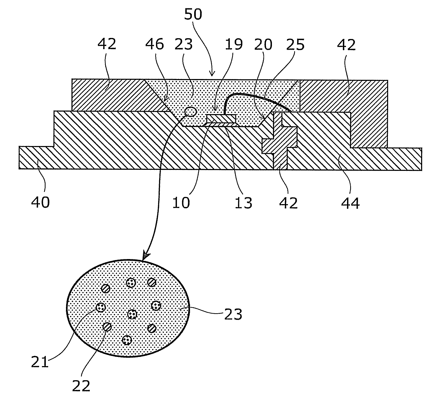
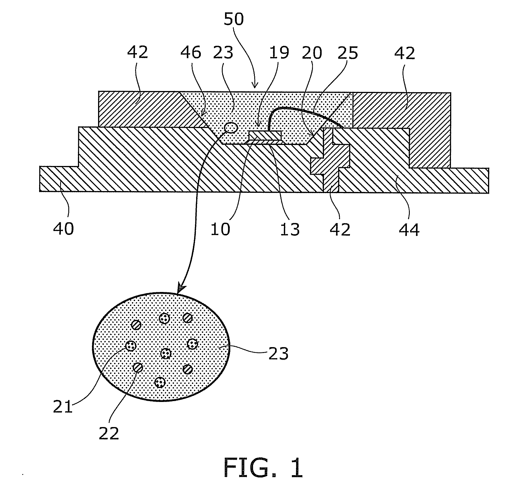
[0024]FIG. 1 is a schematic cross-sectional view showing a semiconductor light emitting device according to the embodiment of the invention. A semiconductor light emitting element 10 is bonded onto a first lead 40 with silver paste 13 or the like. The first lead 40 is provided with a first recess 19. The semiconductor light emitting element 10 is bonded to the bottom surface of the first recess 19.

[0025]An electrode provided on the upper surface of the semiconductor light emitting element 10 is connected to a second lead 44 by a bonding wire 25. The first lead 40 and the second lead 44, made of metal, are buried with a thermoplastic resin 42, for example.

[0026]In the upper portion of the thermoplastic resin 42, a second recess 50 is provided so as to continue to the first recess 19. Inside the thermoplastic resin 42, a sloped reflector 46 is provided. The reflector 46 and the inner sidewall 20 ...


PUM


Abstract

A semiconductor light emitting device includes: a semiconductor light emitting element; a first phosphor which absorbs light emitted from the semiconductor light emitting element and emits first wavelength-converted light; and a second phosphor which absorbs light emitted from the semiconductor light emitting element and emits second wavelength-converted light. The first phosphor has a first excitation spectrum region where excitation intensity increases with increasing wavelength around a peak wavelength of the semiconductor light emitting element. The second phosphor has a second excitation spectrum region where excitation intensity is flat or decreases with respect to increasing wavelength around the peak wavelength of the semiconductor light emitting element.

Description

CROSS-REFERENCE TO RELATED APPLICATIONS[0001]This application is based upon and claims the benefit of priorities from the prior Japanese Application No. 2006-296620, file on Oct. 31, 2006, and the prior Japanese Application No. 2007-274192, file on Oct. 22, 2007; the entire contents of which are incorporated herein by reference.BACKGROUND OF THE INVENTION[0002]1. Field of the Invention[0003]This invention relates to a semiconductor light emitting device.[0004]2. Background Art[0005]The semiconductor light emitting device, which emits mixed color of blue light from a nitride semiconductor light emitting element and yellow light obtained through wavelength conversion by phosphors, is finding wide application in displays, illuminations, and display backlights.[0006]The semiconductor light emitting element includes a quantum well structure made of compound semiconductor thin films. It is not easy to control the composition and thickness of a heterojunction of compound semiconductor thin...

Claims


Application Information

Patent Timeline
IPC IPC(8): H01J1/62H01L33/32H01L33/50H01L33/56H01L33/60H01L33/62
CPCC09K11/7734C09K11/7774H05B33/14H01L2224/32257H01L2224/73265H01L2224/48091H01L2924/00014C09K11/77342
Inventor OTSUKA, KAZUAKI
Owner SEOUL SEMICONDUCTOR
Why Eureka
Try Eureka