High-frequency amplification circuit

a high-frequency amplification and circuit technology, applied in the field of amplifier circuits, can solve the problems of increasing noise factor increasing noise factor, etc., and achieve the effect of high gain, reducing reflection characteristic, and increasing the frequency of desired

Active Publication Date: 2008-06-05
NEC CORP
View PDF6 Cites 1 Cited by
  • Summary
  • Abstract
  • Description
  • Claims
  • Application Information

AI Technical Summary

Benefits of technology

[0012]Accordingly, it is an object of the present invention to provide a high-frequency amplification circuit or a low-noise amplifier (LNA) whose amplification circuit is adapted to a wide band and which has low NF, a small size and low power consumption.

Problems solved by technology

However, there has never been a wide-band wireless communication at a frequency approximately three times the lower limit frequency, i.e., over three octaves.
However, the resistance matching amplification circuit should face a problem of an increased noise factor (NF), the negative feedback amplification circuit should face a problem of an increase in NF and gain reduction, and the traveling-wave amplification circuit should face a problem that the size of the distribution line would increase.
When a signal in a wide band ranging from 3.1 GHz to 10.6 GHz is amplified with low noise, however, the resistance matching amplification circuit, the negative feedback amplification circuit and the traveling-wave amplification circuit have the problems of an increase in NF, gain reduction and an increase in size.

Method used


Image

  • High-frequency amplification circuit
  • High-frequency amplification circuit
  • High-frequency amplification circuit

Examples


Embodiment Construction

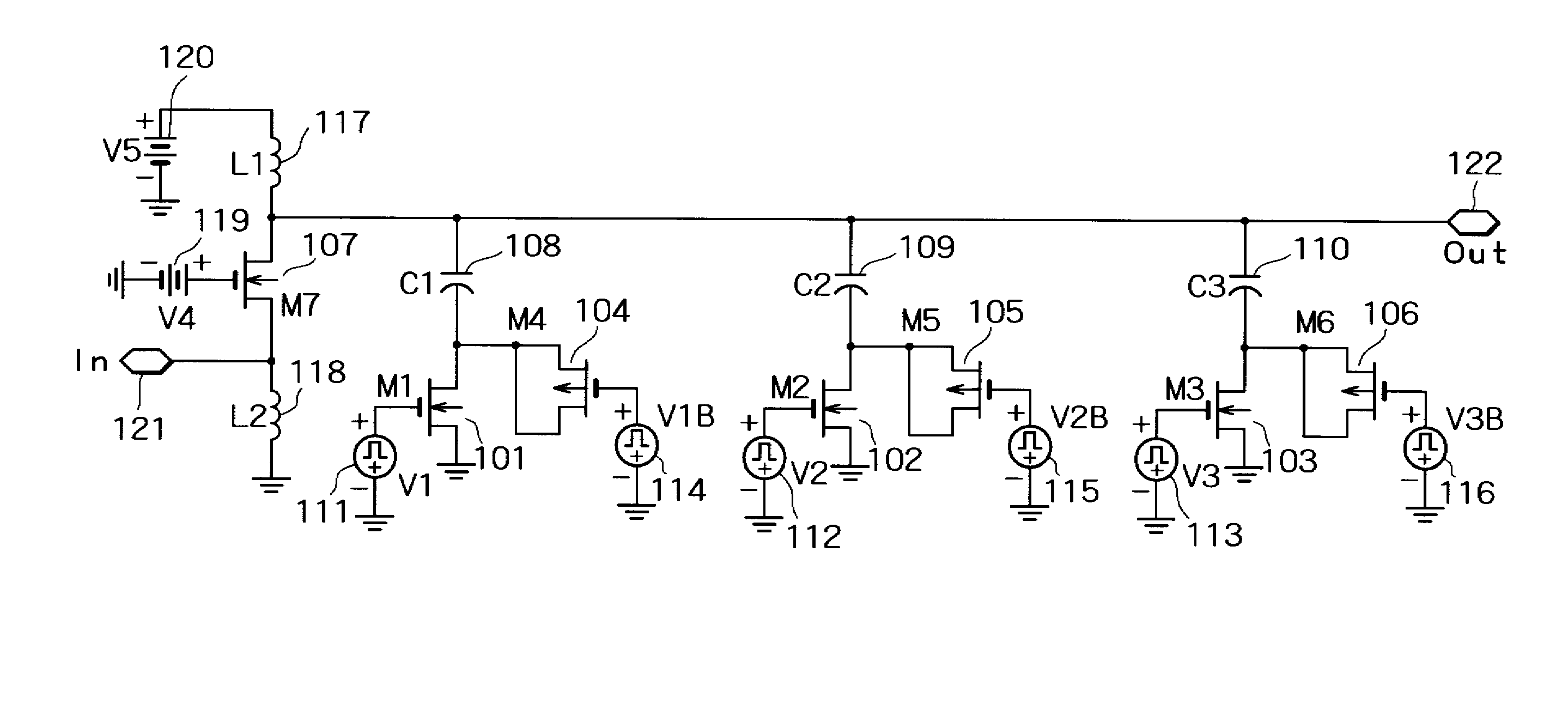
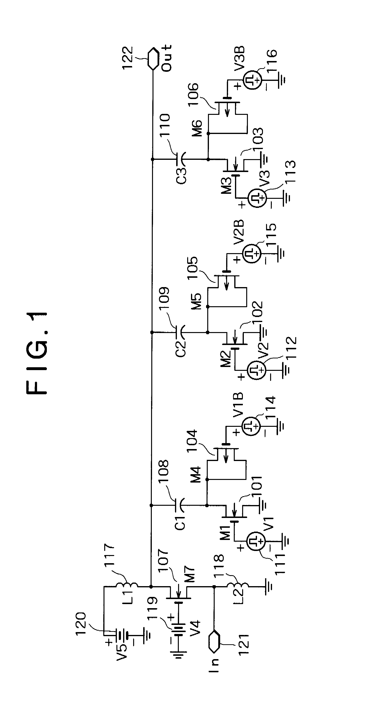
[0068]FIG. 1 is a circuit diagram showing the core portion of a high-frequency amplification circuit according to the first embodiment of the invention. A transistor (M7) 107 is a gate-grounded MOS transistor which constitutes a gate-grounded circuit. A bipolar transistor may be used as the transistor 107 with its base terminal grounded to thereby constitute a gate-grounded circuit. An input signal is input to the source terminal of the transistor 107 from an input terminal 121. An inductor (L2) 118 is connected between the source terminal of the transistor 107 and the ground in order to create the path of the DC bias current. It is preferable that the inductor 118 should have its inductance value increased to such a level that the impedance with respect to an AC signal can be neglected. A wire-bonding inductance element can be used as the inductor 118. A bias voltage 119 connected to the gate of the transistor 107 determines the bias current that flows through the transistor 107. P...


PUM


Abstract

A resonance circuit comprising, for example, an inductor and a plurality of capacitors is provided as a load of a transistor. The capacitors are changed over by a switch. As the capacitors are changed over by the switch, a resonance frequency is changed according to the invention the frequency hopping of an input signal. To cancel ringing that occurs at the time of the switching action, a transistor which cancels gate feed through is added to the switch. An inductor is provided at the gate in order to suppress a gain reduction and an increase in noise factor in a high-frequency range. This provides a compact, wide-band amplifier which has low noise, a wide gain and low power consumption.

Description

BACKGROUND OF THE INVENTION[0001]1. Field of the Invention[0002]The present invention relates to an amplification circuit which amplifies a high-frequency signal, and, more particularly to a wide-band high-frequency amplification circuit which amplifies a signal over a wide frequency band. The high-frequency amplification circuit according to the present invention is adaptable as a wide-band amplification circuit to both wireless communication and cable communication which demand a high transfer rate.[0003]2. Description of the Related Art[0004]Recently, wide-band communication is needed in wireless communication and wide-band communication of 54 Mbps is made into practical use according to the IEEE 802.11a standards. Further, standardization of an ultra wide band (UWB) which is for wireless communication of 1 Gbps class is being made in the IEEE 802.15.TG3a standards. In such wireless communication, the occupied frequency band that is needed for wireless transmission becomes very w...

Claims


Application Information

Patent Timeline
Patent Type & Authority Applications(United States)
IPC IPC(8): H03F3/16H03F3/04H03F3/193H03F1/02H03F1/26H03F1/42H03F3/195
CPCH03F1/02H03F3/195H03F1/42H03F1/26
Inventor TANAKA, AKIO
Owner NEC CORP
Why Eureka
Try Eureka