Supercharge Your Innovation With Domain-Expert AI Agents!

INTEGRATION OF THIN FILM RESISTORS HAVING DIFFERENT TCRs INTO SINGLE DIE

a thin film resistor and single die technology, applied in the direction of solid-state devices, basic electric elements, semiconductor devices, etc., can solve the problems of difficult integrated circuit processing, difficult control of the effect of various thermal cycles on the sheet resistance and tcrs of multiple thin film resistors formed on successive oxide layers, and no practical, economical way to achiev

Active Publication Date: 2008-06-05
TEXAS INSTR INC
View PDF2 Cites 9 Cited by
  • Summary
  • Abstract
  • Description
  • Claims
  • Application Information

AI Technical Summary

Benefits of technology

This approach enables the creation of stable, high-precision thin film resistor structures that can offset negative TCRs of other circuit elements, providing accurate combinations of sheet resistances and TCRs, enhancing the precision and stability of integrated circuit components.

Problems solved by technology

However, there has been no practical, economical way to accomplish this because temperature processing cycles associated with forming subsequent thin film resistor layers subsequent to formation of a first thin film resistor layer would cause a variety of difficult integrated circuit processing problems.
For example, controlling the effect of various thermal cycles on the sheet resistances and TCRs of the multiple thin film resistors formed on successive oxide layers may be very difficult.
Also, the presence of metallization layers in integrated structures including thin film resistors on multiple layers may make it very difficult to design subsequent thermal cycles of the kind needed to be compatible with the thin film resistor properties.
However, there has been no practical way of providing high-precision thin film resistors having positive TCRs in typical integrated circuit structures.
However, the technique of using thermal cycles to obtain a TCR target value that is precisely equal to zero or other value is not practical for some materials and for some sheet resistances, especially for SiCr, and especially for making very low resistance thin film resistors which are very wide and very short and therefore are of substantially reduced accuracy.

Method used


Image

  • INTEGRATION OF THIN FILM RESISTORS HAVING DIFFERENT TCRs INTO SINGLE DIE
  • INTEGRATION OF THIN FILM RESISTORS HAVING DIFFERENT TCRs INTO SINGLE DIE
  • INTEGRATION OF THIN FILM RESISTORS HAVING DIFFERENT TCRs INTO SINGLE DIE

Examples


first embodiment

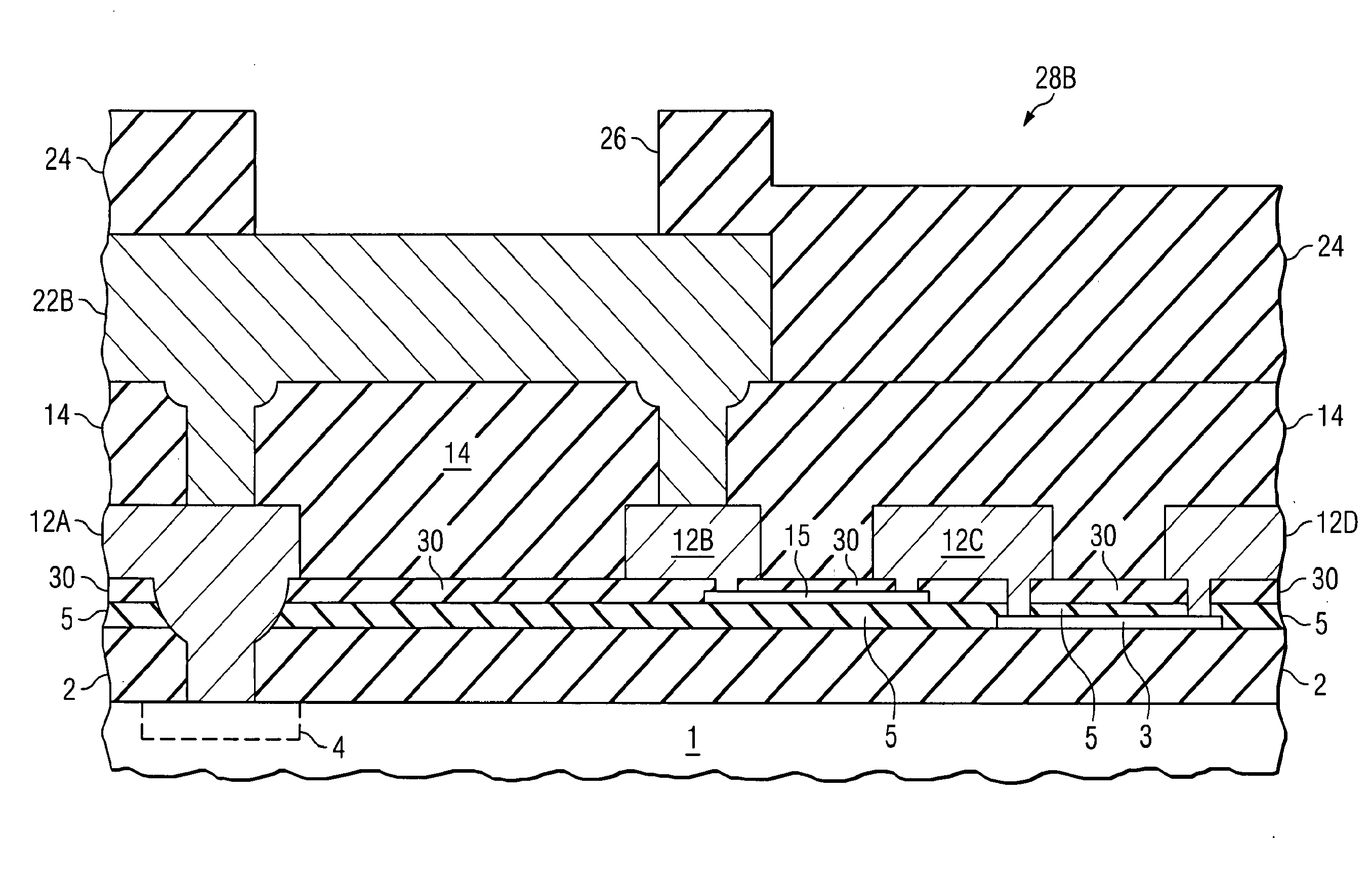
[0023]FIGS. 1-11 illustrate a sequence of processing operations according to the invention for fabricating a first thin film resistor structure including two thin film resistors composed of different thin film material having the same or different sheet resistances and also having the same or different TCRs.

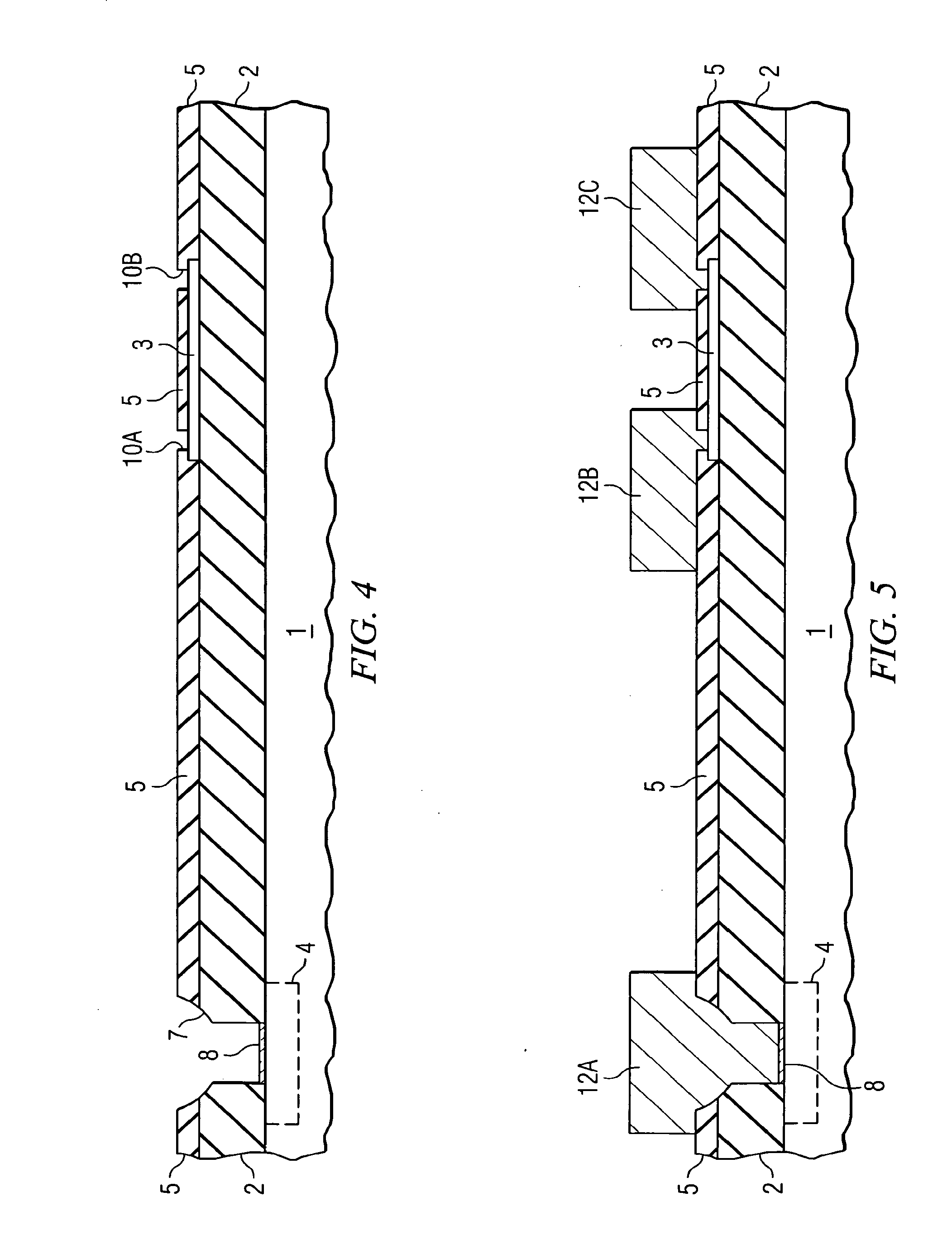
[0024]FIG. 1 shows a starting silicon substrate 1 having a standard pre-metal dielectric layer 2 including a first TEOS (tetraethylorthosilicate) layer on silicon substrate 1, a BPTEOS (Boron-Phosphorus TEOS) layer on the first TEOS sublayer, and a second TEOS layer on the BPTEOS sublayer. A thin layer 3 of sichrome (SiCr) having a sheet resistance, typically in the range from 30 to 2000 ohms per square (based on previously developed curves of TCR versus sheet resistance for the particular SiCr deposition process), has been deposited on the upper surface of pre-metal dielectric layer 2. An anneal process has been performed to adjust the TCR of SiCr layer 3 to a desired (typically...

second embodiment

[0040]In the invention, two different thin film SiCr layers of the same or different sheet resistances and different TCRs are integrated into a structure in which the two different SiCr layers can be interconnected by only the Metal 1 level of interconnect metallization, whereas in the embodiment of FIGS. 1-11, the second SiCr resistor 15 can only be electrically contacted by means of the Metal 2 interconnect metallization layer.

[0041]The same wafer structure with SiCr layer 3 as shown in FIG. 1 is the starting point in making the second embodiment of the invention. FIGS. 12-19 illustrate a sequence of further processing operations according to the second embodiment of the invention for fabricating a thin film resistor structure including two thin film resistors including the same or different sheet resistances and the same or different TCRs, with the ability to adjust the TCR of the lower SiCr layer 3 so as to not affect the subsequently formed upper SiCr layer 15. Referring to FIG...


PUM


Abstract

An integrated circuit structure including multiple thin film resistors having different sheet resistances and TCRs includes a first oxide layer (2) formed on a semiconductor substrate (1), a first thin film resistor (3) disposed on the first oxide layer (2), and a second oxide layer (14) disposed over the first oxide layer (2) and first thin film resistor (3). A second thin film resistor (15) is formed on the second oxide layer (14) and a third oxide layer (16) is formed over the second thin film resistor (15) and the second oxide layer (14). Interconnect metallization elements (12A,B &22A,B) disposed on at least one of the second (14) and third (16) oxide layers electrically contact the circuit element (4), terminals of the first thin film resistor (3), and terminals of the second thin film resistor (15), respectively, through corresponding contact openings through at least one of the second (14) and third (16) oxide layers.

Description

BACKGROUND OF THE INVENTION[0001]The present invention relates generally to practical thin film resistor structures and methods for integrating multiple thin film resistors of the same or different sheet resistances and the same or different temperature coefficients of resistance, and to providing a practical means of adjusting the temperature coefficient of integrated circuit components.[0002]Design engineers would be able to better optimize some integrated circuit designs if it were practical and economical to integrate thin film resistors having various sheet resistances and TCRs (temperature coefficients of resistance) into a single integrated circuit structure. However, there has been no practical, economical way to accomplish this because temperature processing cycles associated with forming subsequent thin film resistor layers subsequent to formation of a first thin film resistor layer would cause a variety of difficult integrated circuit processing problems. For example, con...

Claims


Application Information

Patent Timeline
Patent Type & Authority Applications(United States)
IPC IPC(8): H01L21/4763
CPCH01C1/14H01C7/006H01C7/06H01L28/20H01L21/76804H01L23/5228H01L27/016H01L21/28518H01L2924/0002H01L2924/00
Inventor BEACH, ERIC W.
Owner TEXAS INSTR INC
Features
  • R&D
  • Intellectual Property
  • Life Sciences
  • Materials
  • Tech Scout
  • Unparalleled Data Quality
  • Higher Quality Content
  • 60% Fewer Hallucinations
Learn More