Simulation model making method

a simulation model and modeling method technology, applied in the field of simulation model making, can solve the problems of increasing the difficulty of making a highly precise simulation model, the difficulty of precisely making a physical model that reflects the process effects of a photoresist or the like, and the difficulty of achieving the effect of reducing the difficulty of aging

Inactive Publication Date: 2008-06-05
KK TOSHIBA
View PDF14 Cites 34 Cited by
  • Summary
  • Abstract
  • Description
  • Claims
  • Application Information

AI Technical Summary

Problems solved by technology

As circuit density increases in semiconductor devices, the problem of optical proximity effect (OPE) has become increasingly severe.
It is possible to apply a highly precise physical model to the aerial image calculations; however, it is difficult to precisely make a physical model that reflects the process effects of a photoresist or the like.
Up to now, therefore, it has been difficult to make a highly precise simulation model.
However, merely making a simulation model using a neural network is not enough to perform precise simulation.

Method used


Image

  • Simulation model making method
  • Simulation model making method
  • Simulation model making method

Examples


embodiment 1

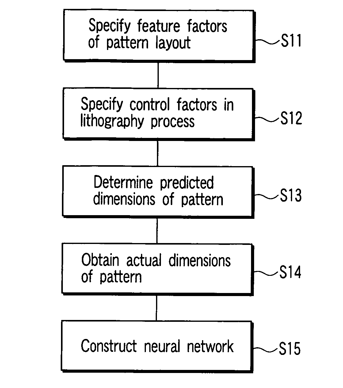
[0020]FIG. 1 is a flowchart which schematically illustrates a method of making a simulation model according to a first embodiment.

[0021]In step S11, feature factors are specified which characterize the pattern layout of a mask pattern. That is to say, feature factors based on pattern layout information are set in a system (a computer or the like) for making a simulation model. The feature factors include target dimensions (pattern widths, space widths, etc.) of the pattern, pattern pitches, the rate of area taken up by the pattern (pattern area rate) within a given region, and the number of patterns within a given region.

[0022]In step S12, control factors are specified which affect the dimensions of the pattern to be formed on a substrate by means of a lithography process. That is, control factors that control the dimensions of the pattern to be formed on a substrate by means of a lithography process are set in the simulation model making system (computer or the like). The control f...

embodiment 2

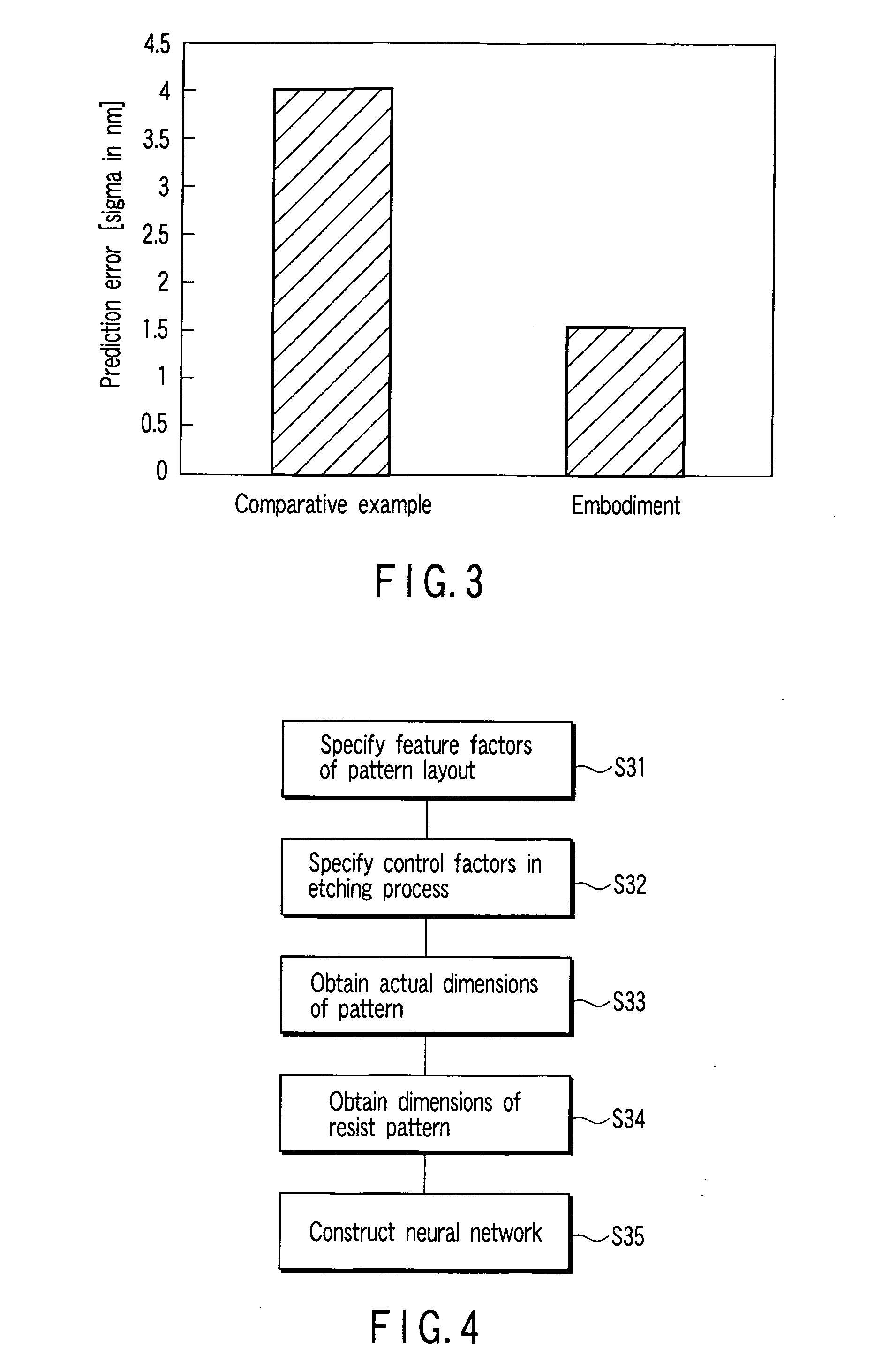
[0035]FIG. 4 is a flowchart which schematically illustrates a method of making a simulation model according to a second embodiment.

[0036]In step S31, feature factors are specified which characterize the pattern layout of a mask pattern. That is to say, feature factors based on pattern layout information are set in a system (a computer or the like) for making a simulation model. The feature factors include target dimensions (pattern widths, space widths, etc.) of the pattern, pattern pitches, the rate of area taken up by the pattern (pattern area rate) within a given region, and the number of patterns within a given region.

[0037]In step S32, control factors are specified which affect the dimensions of the pattern to be formed on a substrate by means of an etching process. That is, control factors that control the dimensions of the pattern to be formed on a substrate by means of an etching process are set in the simulation model making system (computer or the like). Here, the etching ...

embodiment 3

[0045]FIG. 5 is a flowchart which schematically illustrates a method of making a simulation model according to a third embodiment.

[0046]In step S41, a plurality of types of mask patterns is prepared as test patterns used in lithography simulation. Specifically, the mask patterns include line and space patterns, isolated patterns, and island patterns.

[0047]In step S42, the actual dimensions of a resist pattern are obtained which is actually formed on a substrate through a lithography process using a mask pattern. Specifically, the mask pattern is transferred to a photoresist on a semiconductor substrate by means of an exposure apparatus and a development process is then carried out to form the resist pattern. The dimensions of the resist pattern thus actually formed are measured with a scanning electron microscope (SEM). The measured dimensions are entered into a system (a computer or the like) for making a simulation model, and are obtained by the system.

[0048]In step S43, physical ...


PUM

PropertyMeasurementUnit
dimensionaaaaaaaaaa
temperatureaaaaaaaaaa
pressureaaaaaaaaaa

Abstract

A method of making a simulation model, includes specifying a feature factor which characterizes a pattern layout of a mask pattern, specifying a control factor which affects a dimension of a resist pattern to be formed on a substrate by means of a lithography process using the mask pattern, determining a predicted dimension of the resist pattern to be formed on the substrate by means of the lithography process using the mask pattern through the use of a model based on the feature and control factors, obtaining an actual dimension of the resist pattern actually formed on the substrate by means of the lithography process using the mask pattern, and setting the feature and control factors and the predicted dimension as input layers and setting the actual dimension as an output layer to construct a neural network.

Description

CROSS-REFERENCE TO RELATED APPLICATIONS[0001]This application is based upon and claims the benefit of priority from prior Japanese Patent Applications No. 2006-286914, filed Oct. 20, 2006; and No. 2007-245064, filed Sep. 21, 2007, the entire contents of both of which are incorporated herein by reference.BACKGROUND OF THE INVENTION[0002]1. Field of the Invention[0003]The present invention relates to a method of making a simulation model.[0004]2. Description of the Related Art[0005]As circuit density increases in semiconductor devices, the problem of optical proximity effect (OPE) has become increasingly severe. In order to compensate for variations in pattern dimensions due to the OPE, it is required to make optical proximity correction (OPC) on the mask pattern.[0006]To make OPC, it is important to predict the effects of OPE in advance. Usually, lithography simulation is used for this prediction. The lithography simulation involves aerial image calculations based on diffraction theo...

Claims


Application Information

Patent Timeline
Patent Type & Authority Applications(United States)
IPC IPC(8): G06F17/50G03F1/36G03F1/68H01L21/3065
CPCG03F7/70425G03F7/70616G03F7/705G03F7/70491
Inventor ASANO, MASAFUMISATAKE, MASAKITANAKA, SATOSHI
Owner KK TOSHIBA
Why Eureka
Try Eureka