

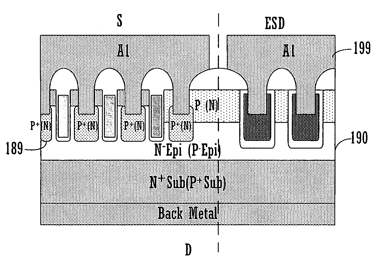
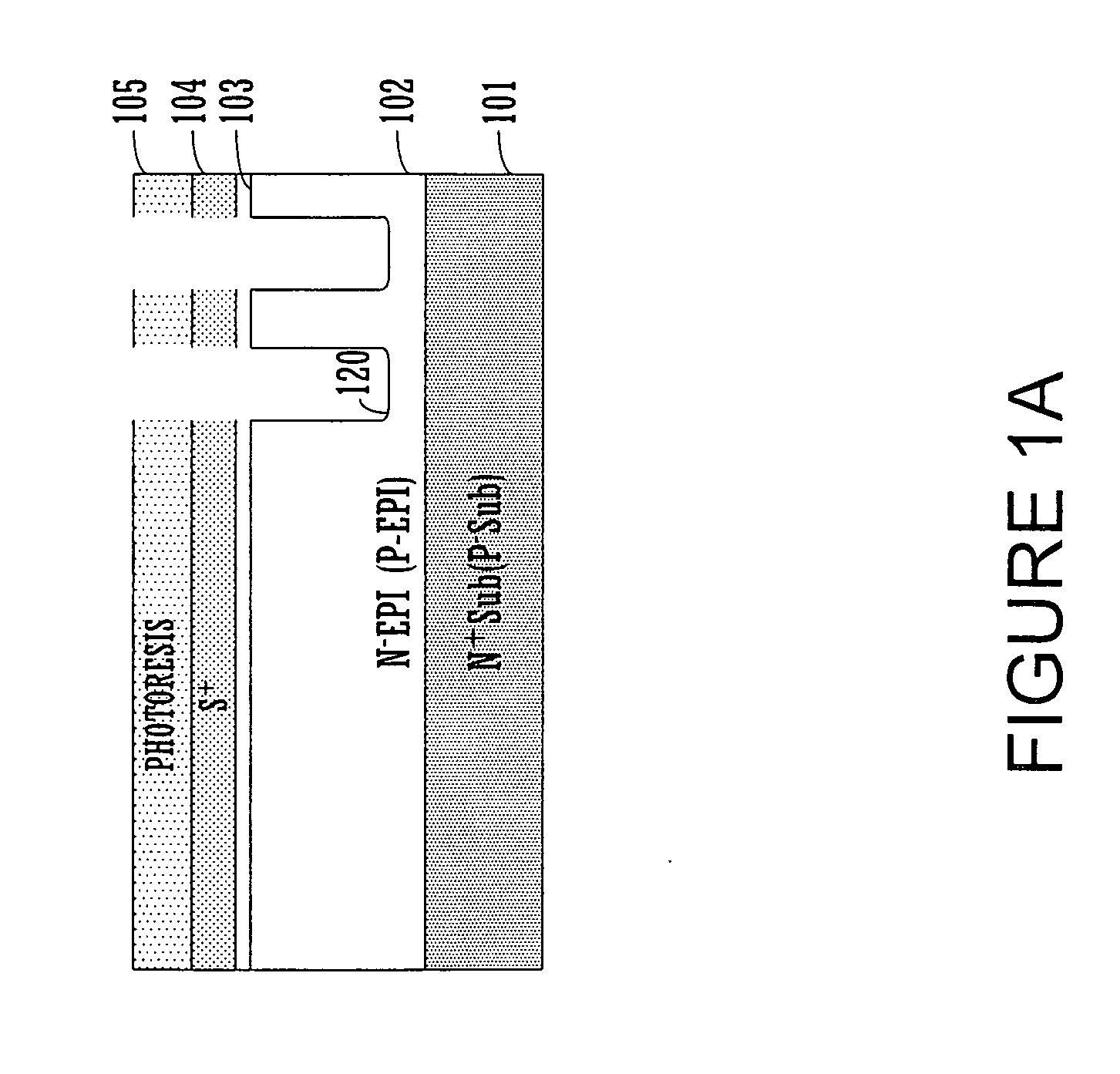
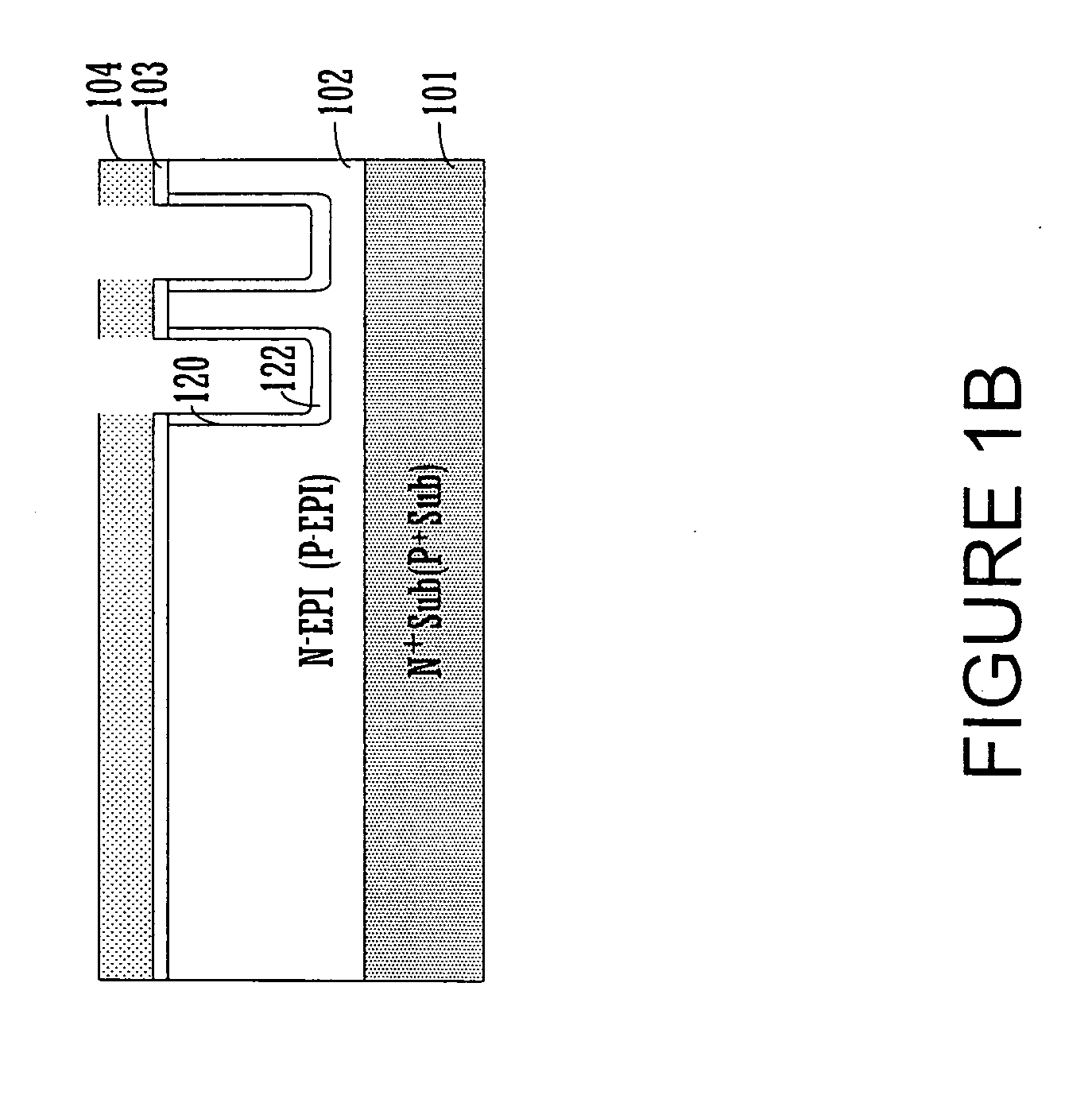
Trench polysilicon diode
a polysilicon diode and polysilicon technology, applied in the direction of diodes, semiconductor/solid-state device details, semiconductors, etc., can solve the problems of many abnormal high voltages, damage to devices, and the inability of the gate oxide layer to withstand high voltage and break down, so as to reduce the topology of the silicon surface, increase the topology of the silicon, and reduce the feature density
- Summary
- Abstract
- Description
- Claims
- Application Information
AI Technical Summary
Benefits of technology
Problems solved by technology
Method used
Image

Examples
Embodiment Construction
[0021]Reference will now be made in detail to the various embodiments of the present invention, examples of which are illustrated in the accompanying drawings. While the invention will be described in conjunction with these embodiments, it will be understood that they are not intended to limit the invention to these embodiments. On the contrary, the invention is intended to cover alternatives, modifications and equivalents, which may be included within the spirit and scope of the invention as defined by the appended claims.
[0022]Furthermore, in the following detailed description of present invention, numerous specific details are set forth in order to provide a thorough understanding of the present invention. However, it will be understood that the present invention may be practiced without these specific details. In other instances, well-known methods, procedures, components, and circuits have not been described in detail so as not to unnecessarily obscure aspects of the present in...
PUM
 Abstract
Description
Claims
Application Information