Method of Manufacturing flash memory device

a technology of flash memory and manufacturing method, which is applied in the direction of semiconductor devices, basic electric elements, electrical appliances, etc., can solve the problems of increased leakage current of high voltage transistors in the peripheral region, hump characteristic generation, and high voltage transistor malfunctions, etc., and achieve the effect of reducing a step

Inactive Publication Date: 2008-04-03
SK HYNIX INC
View PDF4 Cites 2 Cited by
  • Summary
  • Abstract
  • Description
  • Claims
  • Application Information

AI Technical Summary

Benefits of technology

[0006]Accordingly, the present invention discloses a method of manufacturing a non-volatile memory device, in which it can reduce a step between a cell region and a peripheral region in such a manner that the amount of a hard mask, which is lost at the time of etching, can be compensated for by thickly forming the hard mask when a gate is laminated.

Problems solved by technology

It results in an increased leakage current of a high voltage transistor of the peripheral region.
Furthermore, a hump characteristic is generated due to the leakage current, and malfunction of the high voltage transistor may occur due to variation in the threshold voltage of the high voltage transistor.

Method used


Image

  • Method of Manufacturing flash memory device
  • Method of Manufacturing flash memory device
  • Method of Manufacturing flash memory device

Examples


Embodiment Construction

[0010]A specific embodiment according to the present patent will be described with reference to the accompanying drawings.

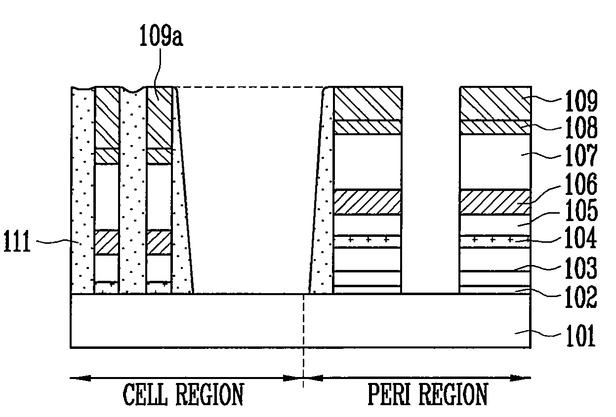
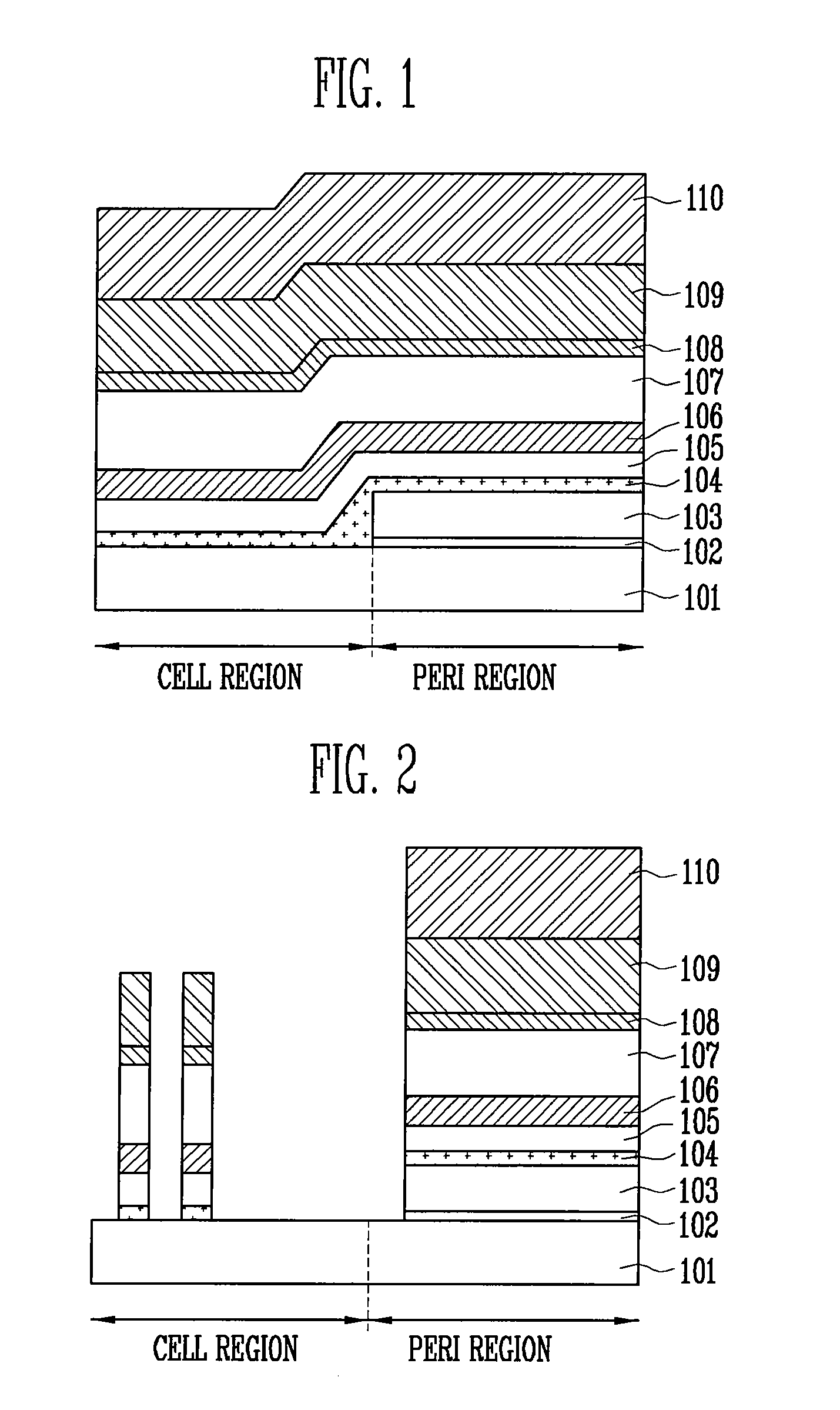
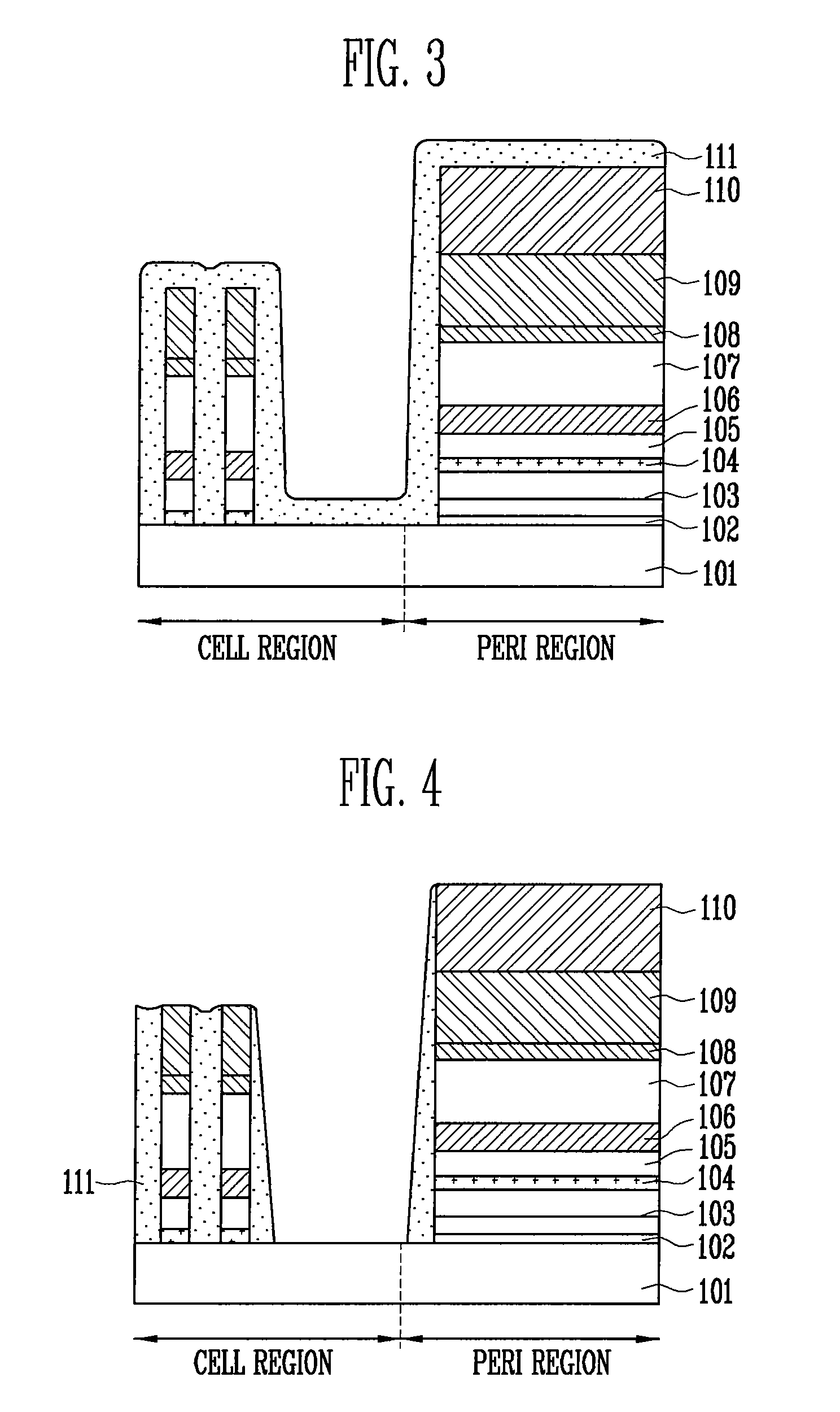
[0011]Referring to FIG. 1, a gate insulating layer 102 and a first conductive layer 103 are formed in a peripheral region of a semiconductor substrate 101. A dielectric layer 104, a capping polysilicon layer 105, a second conductive layer 106, a tungsten silicide layer 107, a SiON layer 108, a hard mask 109 and a carbon hard mask 110 are sequentially laminated over the semiconductor substrate including the first conductive layer 103. The first conductive layer 103 and the second conductive layer 106 are formed from polysilicon. The gate insulating layer 102 and the first conductive layer 103 can be formed to a thickness of about 70 and 800 angstroms, respectively. Furthermore, the dielectric layer 104 can have an ONO (oxide-nitride-oxide) structure. The ONO structure comprises a lamination structure of a lower oxide layer, a nitride layer and an upper oxide layer...


PUM


Abstract

A method of manufacturing a non-volatile memory device includes forming a conductive layer to form a gate on a semiconductor substrate; forming a hard mask over the conductive layer; patterning the hard mask and the conductive layer of a cell region to form the gate; partially recessing the hard mask using a mask through which a peripheral region is opened; and patterning the recessed hard mask and the conductive layer of the peripheral region to form the gate.

Description

CROSS-REFERENCES TO RELATED APPLICATIONS[0001]The present application claims priority to Korean patent application number 10-2006-96011, filed on Sep. 29, 2006, which is incorporated by reference in its entirety.BACKGROUND OF THE INVENTION[0002]The present invention relates to non-volatile memory devices and, more particularly, to a method of manufacturing a non-volatile memory device with a reduced step between a cell region and a peripheral region.[0003]In general, a non-volatile memory device does not lose information even though the supply of power is turned off. Non-volatile memory devices generally include Electrically Programmable Read Only Memory (EPROM), Electrically Erasable and Programmable Read Only Memory (EEPROM), flash EEPROM and so on. In recent years, memory has been formed to have a Silicon / Oxide / Nitride / Oxide / Silicon (SONOS) structure having a three-layered gate insulating layer of an oxide layer / a nitride layer / an oxide layer. If this SONOS structure is used, a n...

Claims


Application Information

Patent Timeline
Patent Type & Authority Applications(United States)
IPC IPC(8): H01L21/3205
CPCH01L27/105H01L27/11573H01L27/11546H01L27/11526H10B41/49H10B41/40H10B43/40
Inventor KIM, SE HOON
Owner SK HYNIX INC
Why Eureka
Try Eureka