Bipolar high electron mobility transistor and methods of forming same

a high electron mobility, transistor technology, applied in transistors, electrical devices, semiconductor devices, etc., can solve the problems of reducing the breakdown voltage of the transistor, significant device processing challenges, and extremely difficult to produce the combined epilayer structure of the bihemt, so as to reduce the minimum sheet resistance limit, and increase the maximum doping

Inactive Publication Date: 2012-12-27
IQE KC
View PDF3 Cites 25 Cited by
  • Summary
  • Abstract
  • Description
  • Claims
  • Application Information

AI Technical Summary

Benefits of technology

[0011]The present invention also provides methods for forming a bipolar high electron mobility transistor whereby a heterojunction bipolar transistor is formed over a field effect transistor; wherein the collector layer is doped with Sn, Te, or Se. In a preferred embodiment, these layers are formed by metalorganic chemical vapor deposition.
[0012]The present invention provides structures and methods to increase the maximum doping and decrease the minimum sheet resistance limits of the collector and / or subcollector of the BiHEMT structures. By doping the collector and subcollector layers with Sn, Te, or Se, including combinations of these, the negative impact due to sheet resistance and electron concentration degradation of GaAs:Si layers can be mitigated. The resultant BiHEMT devices can exhibit reduced subcollector thickness, enabling reduced topology and improved device processing, while preserving the desired low collector sheet resistance.

Problems solved by technology

The combined epilayer structure of a BiHEMT is extremely challenging to produce and can include more than thirty discrete layers.
This leads to significant device processing challenges due to a large height difference (typically 1-3 μm) between the pHEMT surface and the HBT surface.
Although it is desirable to thin the collector layer, this tends to reduce transistor breakdown voltages and degrades device robustness.

Method used


Image

  • Bipolar high electron mobility transistor and methods of forming same
  • Bipolar high electron mobility transistor and methods of forming same
  • Bipolar high electron mobility transistor and methods of forming same

Examples


Embodiment Construction

[0018]A description of example embodiments of the invention follows.

[0019]While this invention has been particularly shown and described with references to example embodiments thereof, it will be understood by those skilled in the art that various changes in form and details may be made therein without departing from the scope of the invention encompassed by the appended claims.

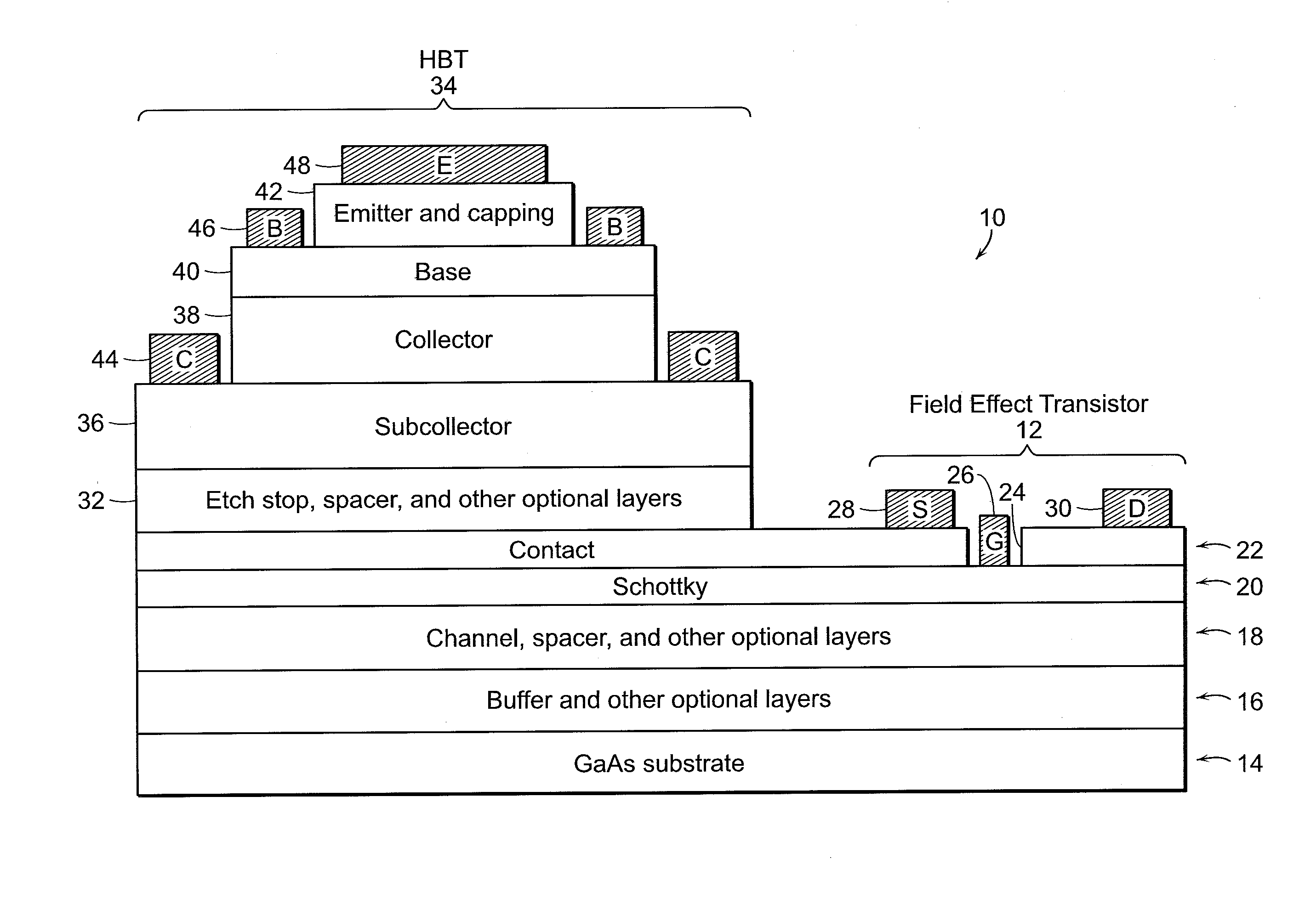
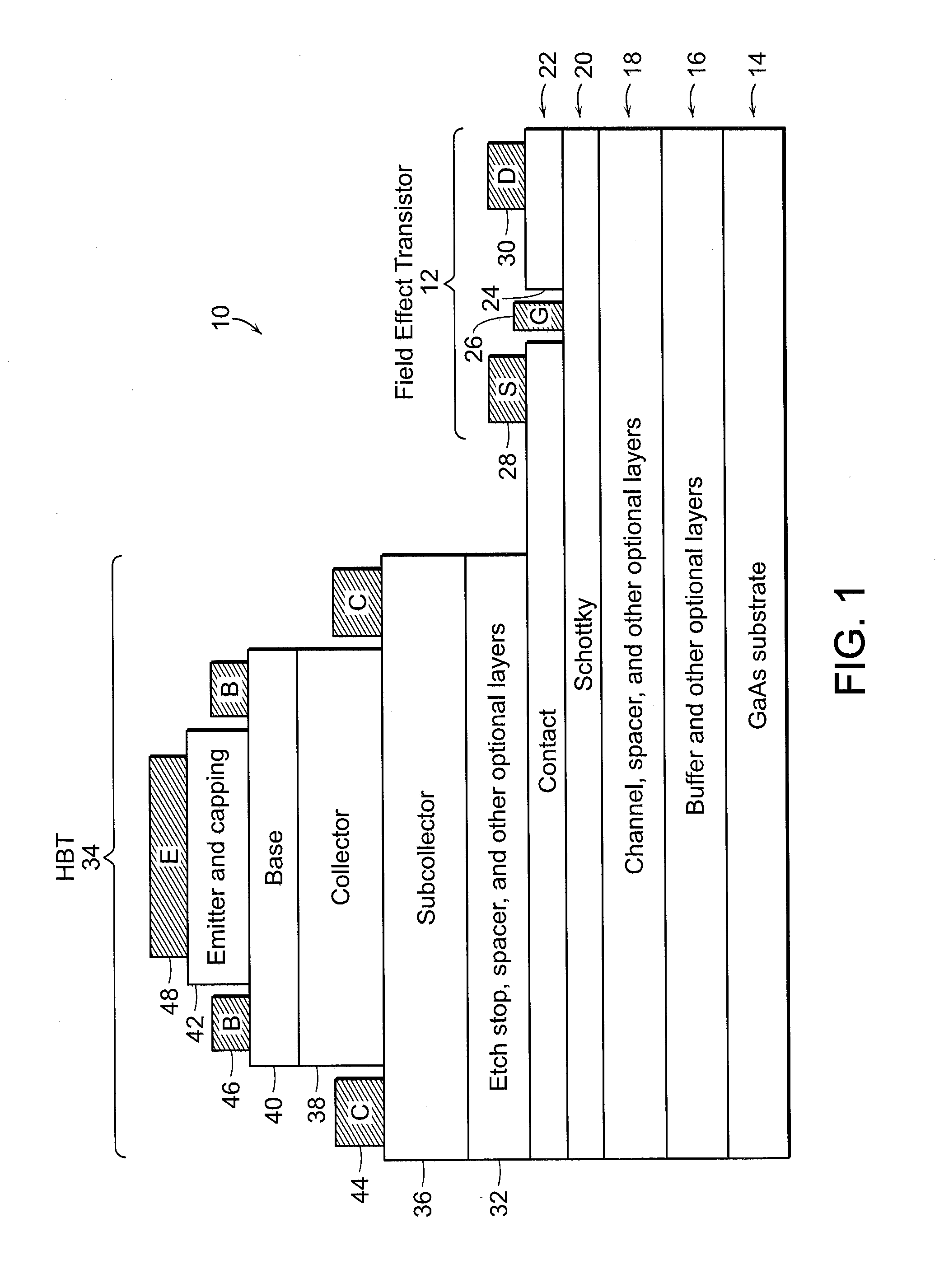
[0020]FIG. 1 is a schematic of a representative BiHEMT epilayer structure of the invention. Note that the layers of the HBT are removed during device fabrication to form the pHEMT on underlying layers. This results in significant topology between the surface of the HBT and the pHEMT. Such topology can cause problems during lithographic steps, particularly those for the pHEMT. For pHEMT switches, the smallest feature is typically the gate electrode and precise optics are required to define dimensions of <1 μm. The topology of the BiHEMT wafer can cause nonuniform photoresist thickness and / or depth-of-focus pro...


PUM


Abstract

An epilayer structure includes a field-effect transistor structure and a heterojunction bipolar transistor structure. The heterojunction bipolar transistor structure contains an n-doped subcollector and a collector formed in combination with the field-effect transistor structure, wherein at least a portion of the subcollector or collector contains Sn, Te, or Se. In one embodiment, a base is formed over the collector; and an emitter is formed over the base. The bipolar transistor and the field-effect transistor each independently contain a III-V semiconductor material.

Description

RELATED APPLICATION[0001]This application claims the benefit of U.S. Provisional Application No. 61 / 500,546, filed on Jun. 23, 2011.[0002]The entire teachings of the above application are incorporated herein by reference.BACKGROUND OF THE INVENTION[0003]Gallium arsenide (GaAs) heterojunction bipolar transistor (HBT) integrated circuits have developed into an important technology for a variety of applications, particularly as power amplifiers (PAs) for wireless communications systems. Future needs are expected to require devices with increased levels of integration to improve performance or functionality, reduce footprint size, or decrease cost. One method to achieve such integration is to combine an HBT PA with a Radio frequency (RF) switch formed from a GaAs pseudomorphic high electron mobility transistor (pHEMT).[0004]In order to monolithically integrate the HBT and pHEMT devices, bipolar high electron mobility transistor (BiHEMT) structures have been used. A typical BiHEMT epitax...

Claims


Application Information

Patent Timeline
Patent Type & Authority Applications(United States)
IPC IPC(8): H01L27/06H01L21/8248
CPCH01L21/8252H01L29/7371H01L27/0623H01L29/7786H01L27/0605H01L29/7783
Inventor STEVENS, KEVIN S.LUTZ, CHARLES R.
Owner IQE KC
Why Eureka
Try Eureka