CMOS image sensor and method for manufacturing the same

a technology of metal oxidesemiconductor and image sensor, which is applied in the direction of electrical equipment, semiconductor devices, radio frequency controlled devices, etc., can solve the problem of too large topology of manufactured devices to obtain high quality images, and achieve the effect of reducing topology

Inactive Publication Date: 2009-09-01
DONGBU ELECTRONICS CO LTD
View PDF1 Cites 4 Cited by
  • Summary
  • Abstract
  • Description
  • Claims
  • Application Information

AI Technical Summary

Benefits of technology

[0013]An advantage of the present invention is to provide a CMOS image sensor and a method for manufacturing the same, which reduces topology by employing a nitride layer for passivation as a microlens.

Problems solved by technology

However, this results in a topology of the manufactured device that is too great to obtain a high quality image.

Method used


Image

  • CMOS image sensor and method for manufacturing the same
  • CMOS image sensor and method for manufacturing the same
  • CMOS image sensor and method for manufacturing the same

Examples


Embodiment Construction

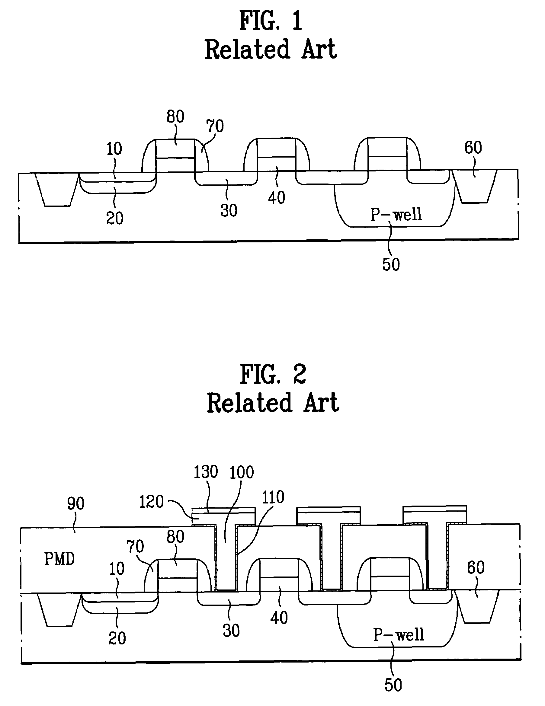
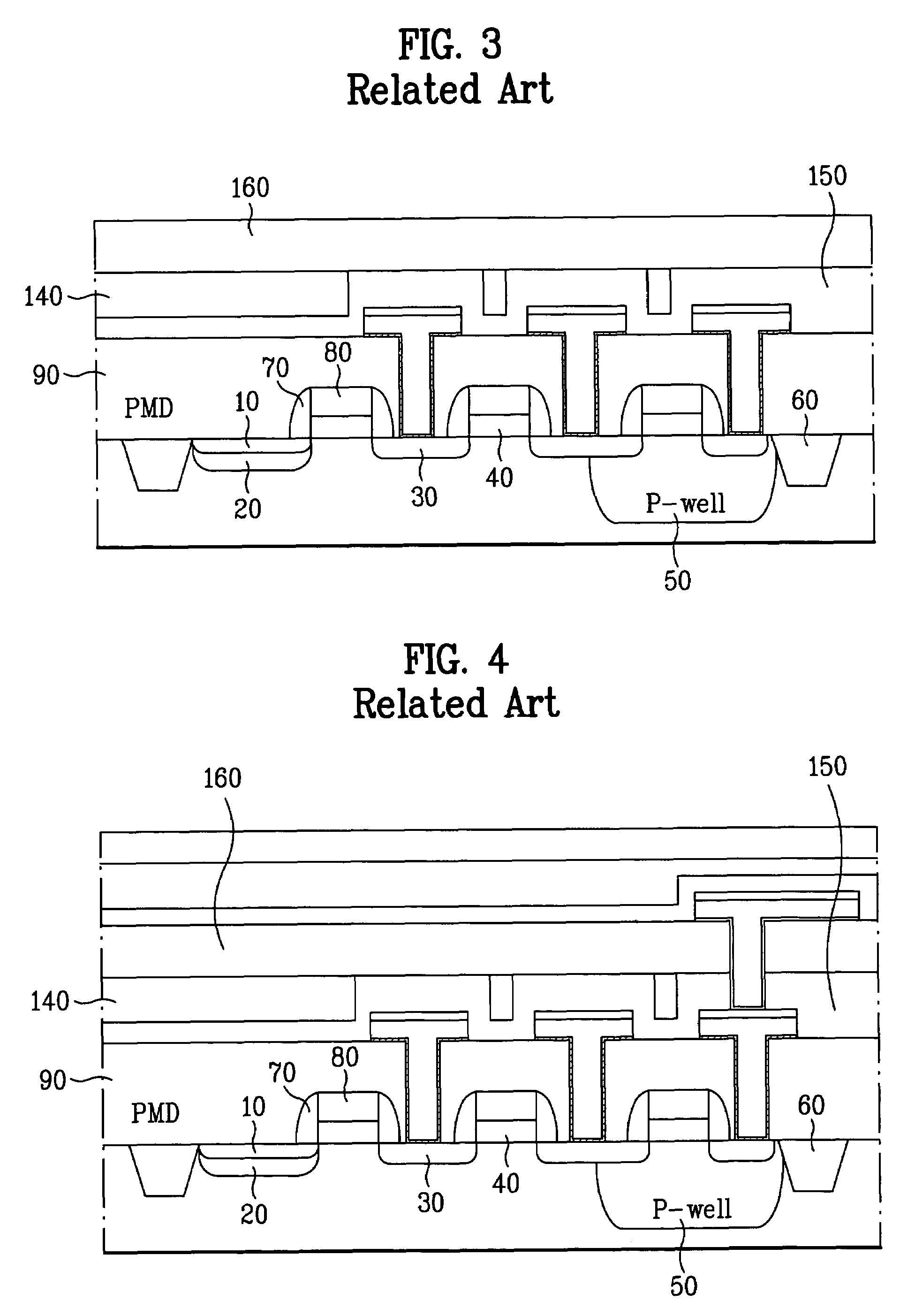
[0021]Reference will now be made in detail to embodiments of the present invention, examples of which are illustrated in the accompanying drawings. Wherever possible, like reference designations will be used throughout the drawings to refer to the same or similar parts.

[0022]FIGS. 7-16 respectively illustrate sequential process steps of a method for fabricating a CMOS image sensor according to the present invention.

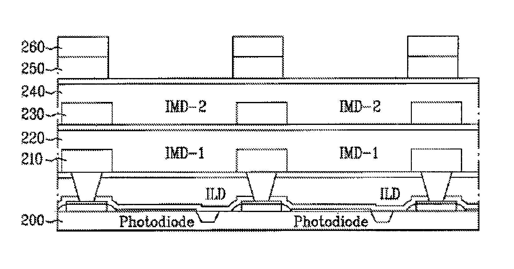
[0023]As shown in FIG. 7, a photodiode 200 is formed. An interlayer dielectric (ILD) layer is formed on the photodiode 200. A first metal layer 210 and a second metal layer 230 are sequentially formed on the ILD layer. A first inter-metal dielectric (IMD-1) layer 220 is formed between the first metal layer 210 and the second metal layer 230. A second inter-metal dielectric (IMD-2) layer 240 is formed on the second metal layer 230. An upper metal layer 250 is partially deposited on the second IMD-2 layer 240. Two upper metal layers 250 are deposited in FIG. 7.

[0024]As show...


PUM

PropertyMeasurementUnit
thicknessaaaaaaaaaa
threshold voltageaaaaaaaaaa
areaaaaaaaaaaa

Abstract

A CMOS image sensor and a method for manufacturing the same are provided, in which a nitride layer for passivation is used as a microlens to reduce topology. The CMOS image sensor includes an upper metal layer partially deposited on a dielectric layer; a first nitride layer deposited on the upper metal layer; an undoped silicon glass layer deposited on the first nitride layer and polished by chemical-mechanical polishing; color filter array elements deposited and exposed on the undoped silicon glass layer and polished by the chemical-mechanical polishing; and a second nitride layer deposited on the first nitride layer and the color filter array elements and transfer-etched after forming a sacrificial microlens on the second nitride layer.

Description

[0001]This application claims the benefit of Korean Patent Application No. 10-2004-0116520, filed on Dec. 30, 2004, which is hereby incorporated by reference for all purposes as if fully set forth herein.BACKGROUND OF THE INVENTION[0002]1. Field of the Invention[0003]The present invention relates to complementary metal-oxide-semiconductor (CMOS) image sensors, and more particularly, to a CMOS image sensor and a method for manufacturing the same, in which a nitride layer for passivation is used as a microlens to reduce topology.[0004]2. Discussion of the Related Art[0005]FIGS. 1-6 respectively illustrate sequential process steps of a method for fabricating a CMOS image sensor according to a related art.[0006]FIG. 1 illustrates a unit pixel region and a peripheral region of a pad, a P-well 50 and an N-well formed by selectively implanting boron ions into a silicon substrate. A field oxide layer 60 is formed by filling a trench using a device isolation process. A gate oxide layer (not ...

Claims


Application Information

Patent Timeline
Patent Type & Authority Patents(United States)
IPC IPC(8): H01L21/00H01L31/062H01L31/113
CPCH01L27/14621H01L27/14685H01L27/14627H01L27/14632H01L27/146H01L31/10
Inventor HAN, CHANG HUN
Owner DONGBU ELECTRONICS CO LTD
Why Eureka
Try Eureka