Method For Encapsulating A Device In A Microcavity

a microcavity and device technology, applied in the field of encapsulation, can solve the problems of affecting the encapsulation process, the device is damaged, and the atmospheric pressure technique does not prevent the material deposition inside the cavity, so as to achieve the effect of increasing the yield or reliability, increasing the protection, and increasing the resistance to gravitational forces

Inactive Publication Date: 2008-06-12
KATHOLIEKE UNIV LEUVEN +1
View PDF9 Cites 46 Cited by
  • Summary
  • Abstract
  • Description
  • Claims
  • Application Information

AI Technical Summary

Benefits of technology

[0013]a) The temperature budget is low. Metal can be deposited at low temperature. A resist step is not required which avoids resist baking. So temperatures during manufacture can be kept to less than 200° C., or even less than 150° C. This is particularly important where the encapsulation is over a cavity for a sensitive part such as a MEMS component whose characteristics should not change.
[0017]e) Can be made with reduced manufacturing complexity by avoiding lithography.
[0018]f) The porous layer can enable removal of the sacrificial layer yet provide more protection against inadvertent contamination of the micro cavity than is provided by conventional etched apertures in metal. This is because the pores can provide more resistance to gravitation driven flow of particles or fluids during sealing or other intermediate steps before sealing, during manufacture. Thus yield or reliability can be increased for devices having sensitive components in the micro cavity.
[0019]If compared to a conventional capping layer where holes are formed by a lithographic step, avoiding a lithographic step is less expensive and is less time consuming. Moreover, the holes conventionally made using lithography are quite “large”, e.g. about 2 micron as making smaller holes by litho is expensive. Thus, during the step of forming the sealing layer, material can fall into the cavity.
[0020]In contrast, the porous layer claimed can form a capping layer that has good mechanical properties and that has small holes (between 10 nm and a few micrometer compared to litho) and can be formed by steps which don't harm a sensitive device such as a MEMS device inside the cavity.

Problems solved by technology

The encapsulation has to be performed without the deposition of sealing material on the MEMS device, which can cause damage to the device.
Moreover, most of these atmospheric pressure techniques do not prevent material deposition inside the cavity.
Etching openings moreover requires patterning, masking steps etc which complicate the whole process of encapsulation.

Method used


Image

  • Method For Encapsulating A Device In A Microcavity
  • Method For Encapsulating A Device In A Microcavity
  • Method For Encapsulating A Device In A Microcavity

Examples


Embodiment Construction

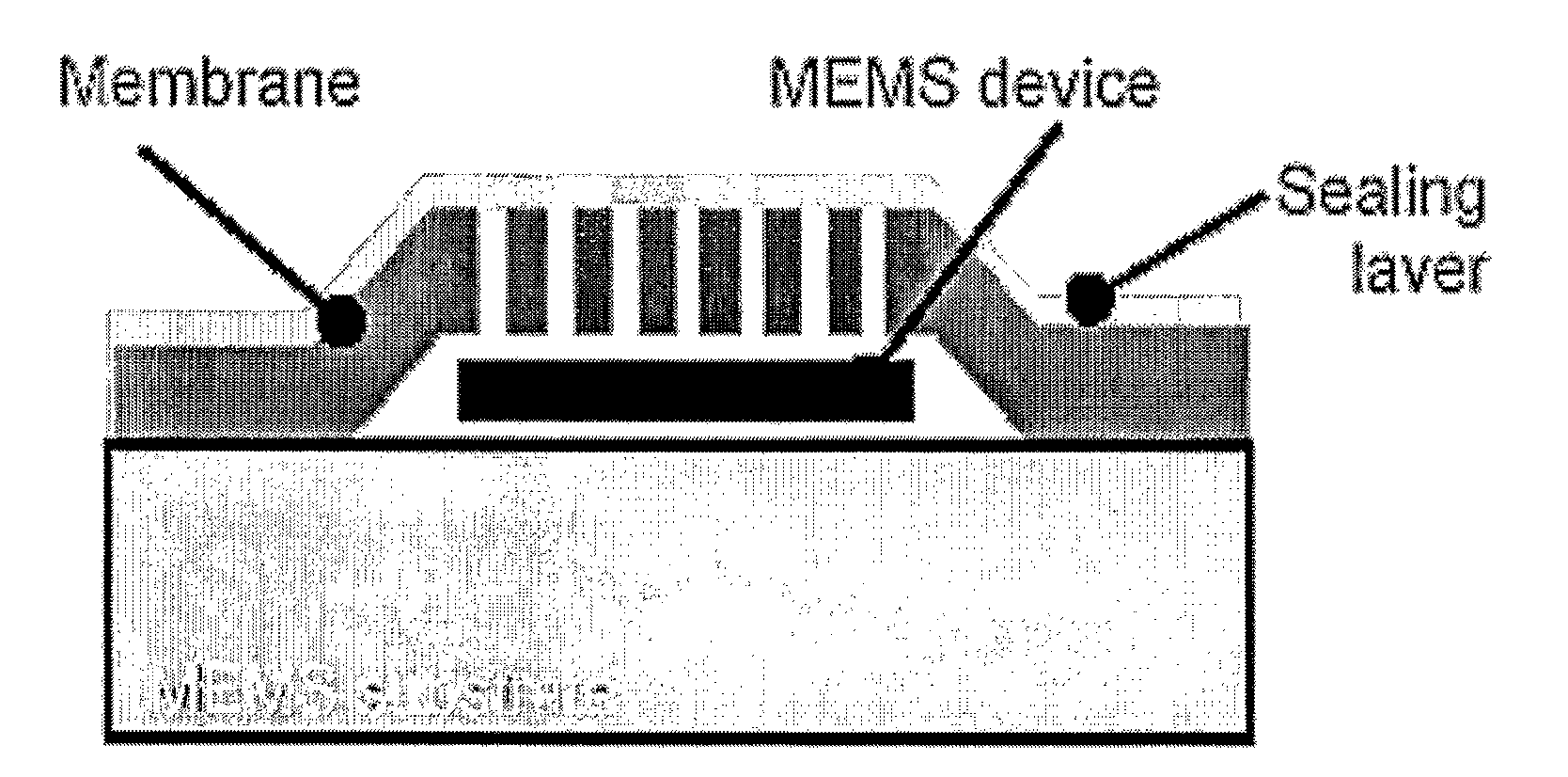
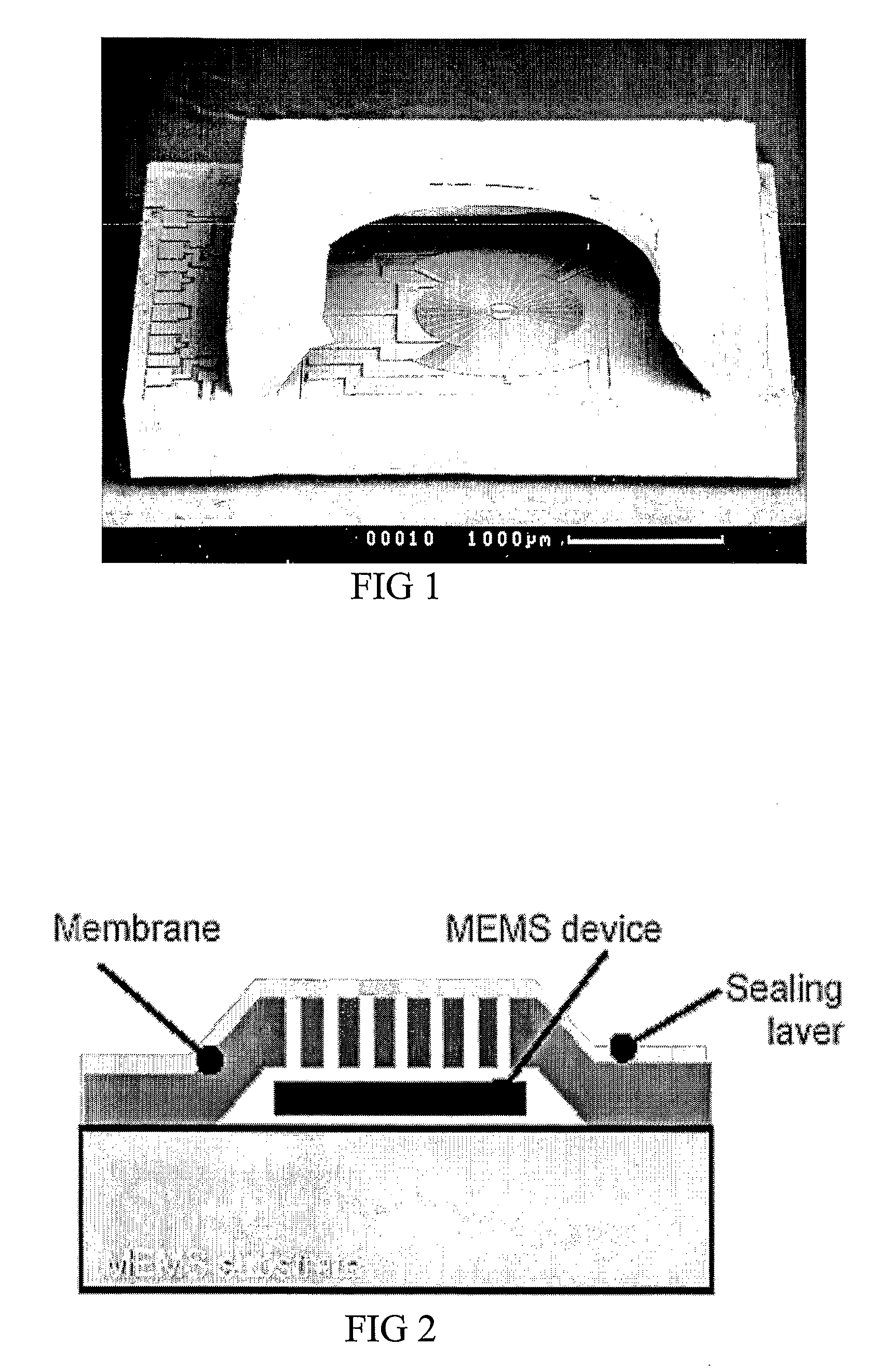
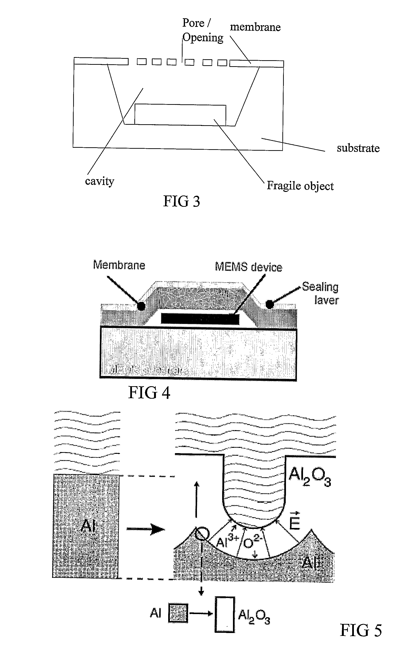
[0048]The present invention will be described with respect to particular embodiments and with reference to certain drawings but the invention is not limited thereto but only by the claims. The drawings described are only schematic and are non-limiting. In the drawings, the size of some of the elements may be exaggerated and not drawn on scale for illustrative purposes. The dimensions and the relative dimensions do not correspond to actual reductions to practice of the invention.

[0049]Furthermore, the terms first, second, third and the like in the description and in the claims, are used for distinguishing between similar elements and not necessarily for describing a sequential or chronological order. It is to be understood that the terms so used are interchangeable under appropriate circumstances and that the embodiments of the invention described herein are capable of operation in other sequences than described or illustrated herein.

[0050]It is to be noticed that the term “comprisin...


PUM

PropertyMeasurementUnit
thicknessaaaaaaaaaa
lengthaaaaaaaaaa
thicknessaaaaaaaaaa

Abstract

Manufacturing a semiconductor device involves forming (200) a sacrificial layer where a micro cavity is to be located, forming (210) a metal layer of thickness greater than 1 micron over the sacrificial layer, forming (220) a porous layer from the metal layer, the porous layer having pores of length greater than ten times their breadth, and having a breadth in the range 10 nm-500 nanometers. The pores can be created by anodising, electrodeposition or dealloying. Then the sacrificial layer can be removed (230) through the porous layer, to form the micro cavity, and pores can be sealed (240). Encapsulating MEMS devices with a porous layer can reduce costs by avoiding using photolithography for shaping the access holes since the sacrificial layer is removed through the porous membrane.

Description

FIELD OF THE INVENTION[0001]The present invention is related to methods of manufacturing semiconductor devices, (especially to methods of encapsulation) and to such devices. Particular embodiments relate to microelectronic process technology, to Micro- and Nano-Electro Mechanical Systems (MEMS and NEMS) process and encapsulation or packaging teclmology, to methods for the O-Level or wafer level packaging or encapsulation objects for instance MEMS devices. Such encapsulation can cause a cavity, in which an object can be located, such as to be hermetically sealed.BACKGROUND[0002]Many micro-electromechanical systems (MEMS) require an encapsulation under vacuum or under a controlled atmosphere and pressure in order to ensure either a good performance or an acceptable lifetime of operation. The encapsulation has to be performed without the deposition of sealing material on the MEMS device, which can cause damage to the device.[0003]The most popular approach is based on wafer bonding. Her...

Claims


Application Information

Patent Timeline
Patent Type & Authority Applications(United States)
IPC IPC(8): H01L21/56H01L23/02
CPCB81C2203/0145B81C1/00293
Inventor WITVROUW, ANNVAN HOOF, CHRISFRANSAER, JANCELIS, JEAN-PIERREMUSCAT, ANTHONY JOSEPHHELLIN RICO, RAQUEL CONSUELO
Owner KATHOLIEKE UNIV LEUVEN
Why Eureka
Try Eureka