
Silicon Oxynitride Coating Compositions

a technology of oxynitride and coating composition, which is applied in the direction of vacuum evaporation coating, coating, lasers, etc., can solve the problems of limiting the operating voltage of dc-field photoelectron guns, emitted electron current, damage to electrode surfaces, etc., and achieves the effect of reducing costs and hazards, and low allowable total thermal budg

Inactive Publication Date: 2009-11-12
COLLEGE OF WILLIAM & MARY
View PDF17 Cites 12 Cited by
  • Summary
  • Abstract
  • Description
  • Claims
  • Application Information

AI Technical Summary

Benefits of technology

The patent describes a method for depositing silicon oxynitride coatings with a controlled amount of nitrogen gas and a low temperature requirement. The coatings can be used in a variety of applications such as semiconductor devices, where they can be used as dielectrics or to suppress field emission. The method uses a low-temperature process and does not require the use of hazardous gases. The coatings can be deposited onto a wide range of substrate materials and can be used as coatings to improve the performance of certain materials.

Problems solved by technology

Currently, field emission from support electrodes limits the operating voltages in DC-field photoelectron guns, which is problematic because operating at higher voltages would increase both the intensity and quality of the output electron beam by increasing the bunch charge and decreasing the divergence of the emitted electrons.
This method drastically reduced the emitted electron current, but numerous arcs occurred during the coating process which severely damaged the electrode surface when this coating process was applied to three dimensional structures, in particular smooth, polished structures similar to those used in DC-field photoelectron guns.
However, transistors that use silicon dioxide as a dielectric have a tendency to leak electrons when the transistor thickness is less than 130 nanometers.

Method used


Image

  • Silicon Oxynitride Coating Compositions
  • Silicon Oxynitride Coating Compositions
  • Silicon Oxynitride Coating Compositions

Examples


example 1

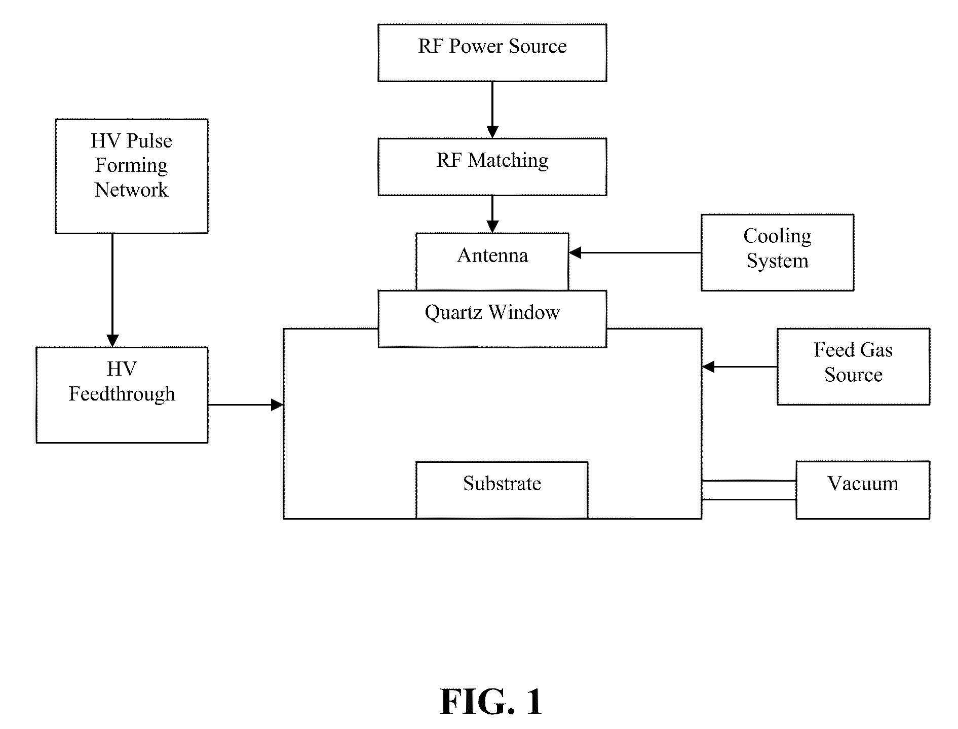
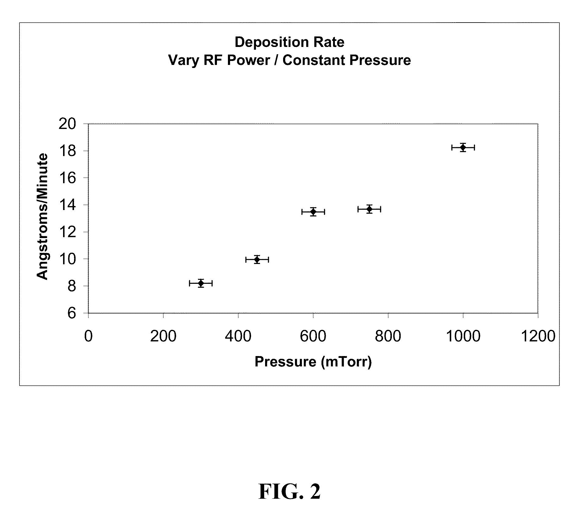
[0044]A set of experiments was performed using 7 mm×7 mm silicon samples that were all cut from the same wafer. Using the General Procedure described above for reactive sputtering, the nitrogen plasma pressure was fixed at 1.7 mTorr while the RF-power was incrementally adjusted. Four silicon samples and two “masked” silicon samples were then coated for 4 hours at each of the following RF power levels: 300 W, 450 W, 600 W, 750 W, and 1 kW incident power, with less than 25 W reflected power in all cases.

[0045]The two masked silicon samples were then analyzed using profilometry to measure the step height, or thickness of the coating. Each sample was analyzed at three different locations, and their corresponding thickness values were averaged. The deposition rate was then calculated by dividing the average thickness by the total process time, namely 240 min. The four other samples were analyzed using FTIR to determine how much Si—N content was present in the silicon oxynitride film. The...

example 2

[0052]A set of experiments was performed using 7 mm×7 mm silicon samples that were all cut from the same wafer. Using the General Procedure described above, the RF-power was fixed at 750 W incident power while the nitrogen plasma pressure was incrementally varied. The reflected RF-power was kept below 25 W. Six samples, comprising four silicon samples and two masked silicon samples, were coated for 4 hours at each of the following nitrogen pressures: 1 mTorr, 1.7 mTorr, 2.5 mTorr, 3.3 mTorr, 4 mTorr, and 5 mTorr. It should be noted that greater pressure ranges can be achieved with different vacuum pumps known in the art; for example, the 16 cfm scroll pump used in the present example could be replaced by a larger, oil-lubricated rotary vane pump, or the 1000 l / s maglev turbo pump used in the present example could be replaced with a smaller turbo pump.

[0053]The two masked silicon samples were then analyzed using profilometry to measure the step height, or thickness of the coating. Ea...

example 3

[0057]Silicon oxynitride coatings were deposited onto 7 mm×7 mm silicon samples using the procedure of Example 1, with a fixed nitrogen pressure of 1.70 mtorr and 750 W incident RF power.

[0058]Atomic CompositionAuger Electron Spectroscopy. The atomic compositions of the silicon oxynitride layers created by the reactive sputtering deposition procedures were obtained using Auger Electron Spectroscopy (AES) with a cylindrical mirror electron energy analyzer having a fixed resolution of 0.6% of the peak energy. Depth profiles were obtained by rastering a 400-500 μm diameter, 3 keV argon ion beam to sputter a 2 mm by 2 mm surface area. The sputter rate was calibrated against that of silicon dioxide, and the relative sensitivity factor treated the silicon as an oxide. FIG. 8 shows the AES depth profile of the reactively sputtered silicon oxynitride films. A layer of silicon, oxygen, and nitrogen was deposited that is roughly 600 nm thick. The concentration of silicon was approximately 30...


PUM

PropertyMeasurementUnit
temperatureaaaaaaaaaa
thicknessaaaaaaaaaa
thicknessaaaaaaaaaa

Abstract

Silicon oxynitride compositions are described herein. These compositions are typically deposited onto substrates using a nitrogen plasma-based, reactive sputtering method. Depending on their composition, these coatings can be used for field emission suppression, dielectric applications, reflection control, and surface passivation.

Description

CROSS-REFERENCE TO RELATED APPLICATIONS[0001]This application is a division (and claims the benefit of priority under 35 U.S.C. 120) of application Ser. No. 11 / 856,814, filed Sep. 18, 2007. The disclosure of the prior application is considered part of, and hereby incorporated by reference, in the disclosure of this application.STATEMENT REGARDING FEDERALLY SPONSORED RESEARCH AND DEVELOPMENT[0002]This invention was made with government support under Grant No. DE-AC05-84ER-40150 awarded by the Department of Energy. The government has certain rights in the invention.FIELD OF INVENTION[0003]This invention relates to silicon oxynitride coatings useful in both low voltage (e.g., semiconductors) and high voltage (e.g., field emission suppression) applications.BACKGROUND OF THE INVENTION[0004]Although certain applications, like vacuum tubes, require materials that emit large currents at low voltages, other high voltage industries require the suppression of field emission. For example, the e...

Claims


Application Information

Patent Timeline
Patent Type & Authority Applications(United States)
IPC IPC(8): C23C14/34
CPCH01S3/02H01S3/0903H01S3/025
Inventor THEODORE, NIMELHOLLOWAY, BRIAN C.MANOS, DENNIS M.
Owner COLLEGE OF WILLIAM & MARY
Learn More