Method of manufacturing metal-oxide-semiconductor transistor

a technology of metal-oxidesemiconductor and semiconductor, which is applied in the direction of transistors, semiconductor devices, electrical equipment, etc., can solve the problems of inability to prevent the diffusion of dopants, the resistance at the source/drain terminal is still relatively high, and the saturated drain current is still relatively low, so as to reduce the resistance of the sheet

Inactive Publication Date: 2005-09-13
UNITED MICROELECTRONICS CORP
View PDF2 Cites 14 Cited by
  • Summary
  • Abstract
  • Description
  • Claims
  • Application Information

AI Technical Summary

Benefits of technology

[0008]Accordingly, one object of the present invention is to provide a method of manufacturing a metal-oxide-semiconductor (MOS) transistor capable of reducing sheet resistance at the source / drain terminal of the transistor.
[0009]A second object of this invention is to provide a method of manufacturing a metal-oxide-semiconductor (MOS) transistor capable of improving the electrical properties of the transistor.
[0013]In this invention, a pre-annealing operation is carried out before the solid phase epitaxial process so that the amorphized region is re-crystallized to form large crystals. Hence, sheet resistance at the source / drain terminal of the MOS transistor is greatly reduced.
[0014]Furthermore, a post-annealing operation is carried out after the solid phase epitaxial process so that the distance between the source / drain region and the extension region of the transistor is reduced. Thus, the electrical performance of the transistor is greatly improved.
[0015]In addition, the MOS transistor of this invention utilizes a solid phase epitaxial process to activate the dopants within the source / drain region. Since the solid phase epitaxial process has a low thermal budget, transition stage acceleration and short channel effect resulting from using a high-temperature annealing process can be prevented.

Problems solved by technology

The annealing operation is carried out a high temperature of between 800° C. to 900° C. Although the pre-amorphization implantation is able to lower the channel effect due to the dopants, the diffusion of dopants cannot be prevented.
However, the resistance at the source / drain terminal is still relatively high and the saturated drain current is still relatively low for a MOS transistor fabricated using this method.

Method used


Image

  • Method of manufacturing metal-oxide-semiconductor transistor
  • Method of manufacturing metal-oxide-semiconductor transistor
  • Method of manufacturing metal-oxide-semiconductor transistor

Examples


Embodiment Construction

[0022]Reference will now be made in detail to the present preferred embodiments of the invention, examples of which are illustrated in the accompanying drawings. Wherever possible, the same reference numbers are used in the drawings and the description to refer to the same or like parts.

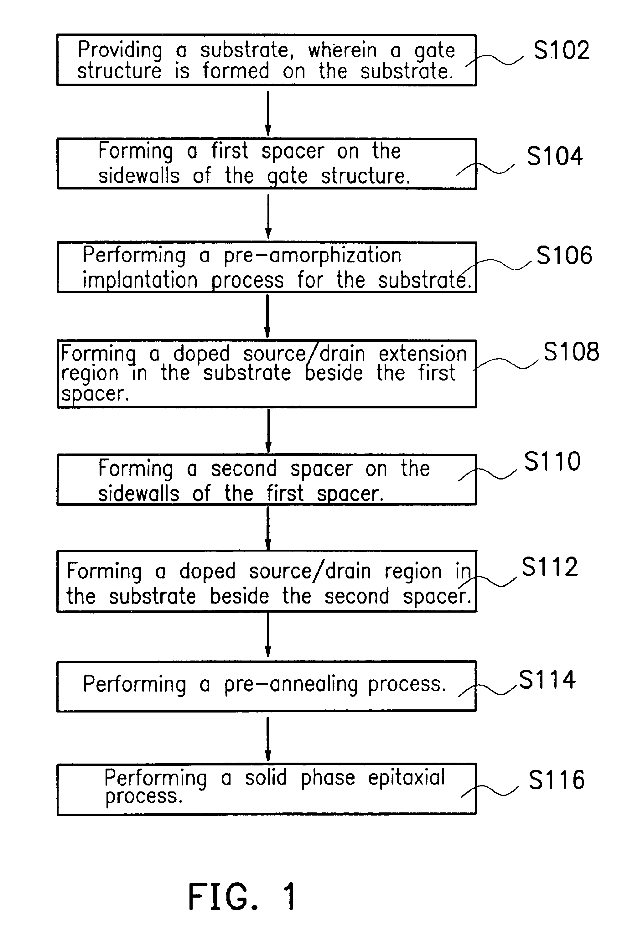
[0023]FIG. 1 is a flowchart showing the steps for fabricating a metal-oxide-semiconductor transistor according to a first preferred embodiment of this invention.

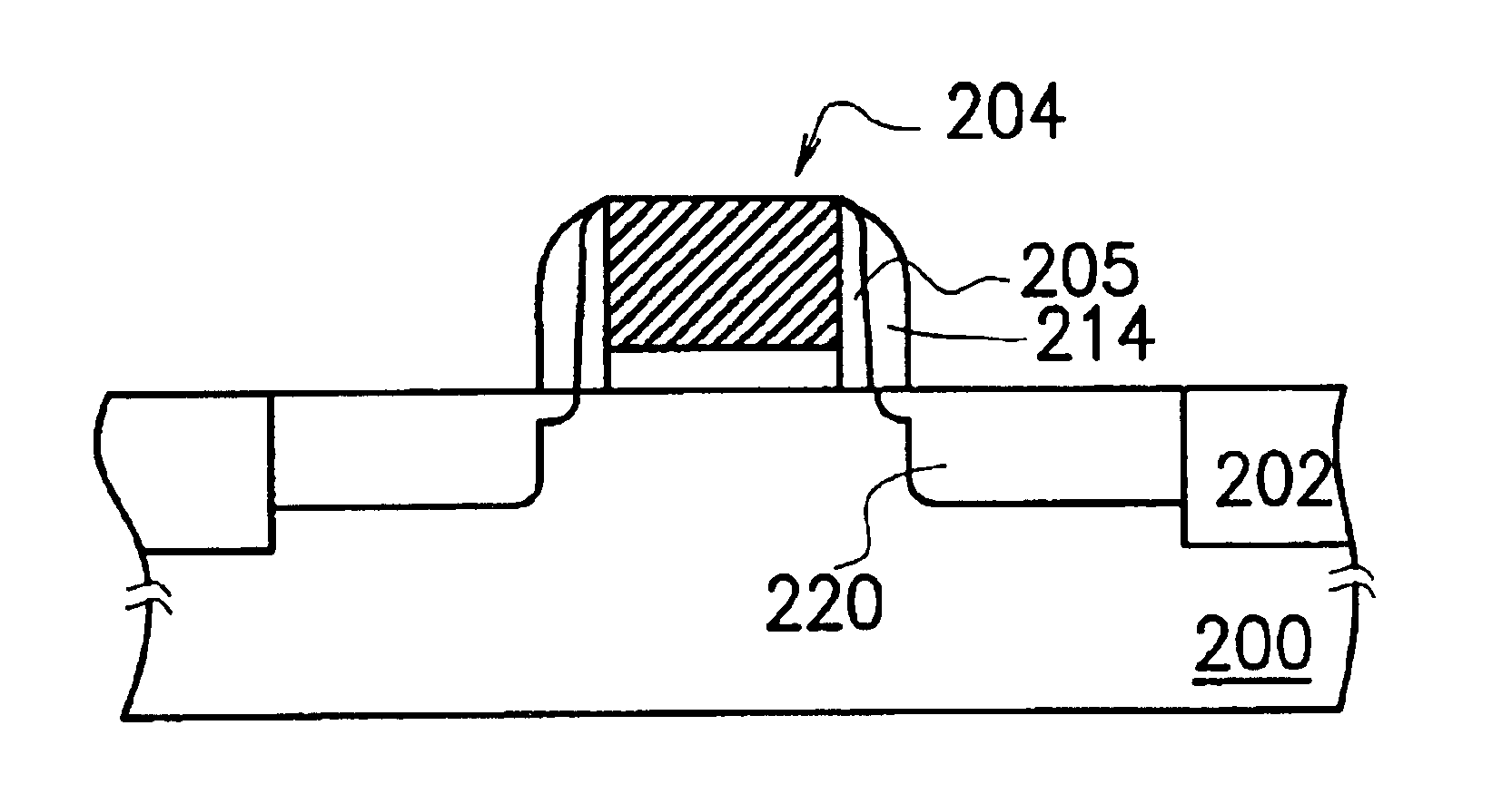
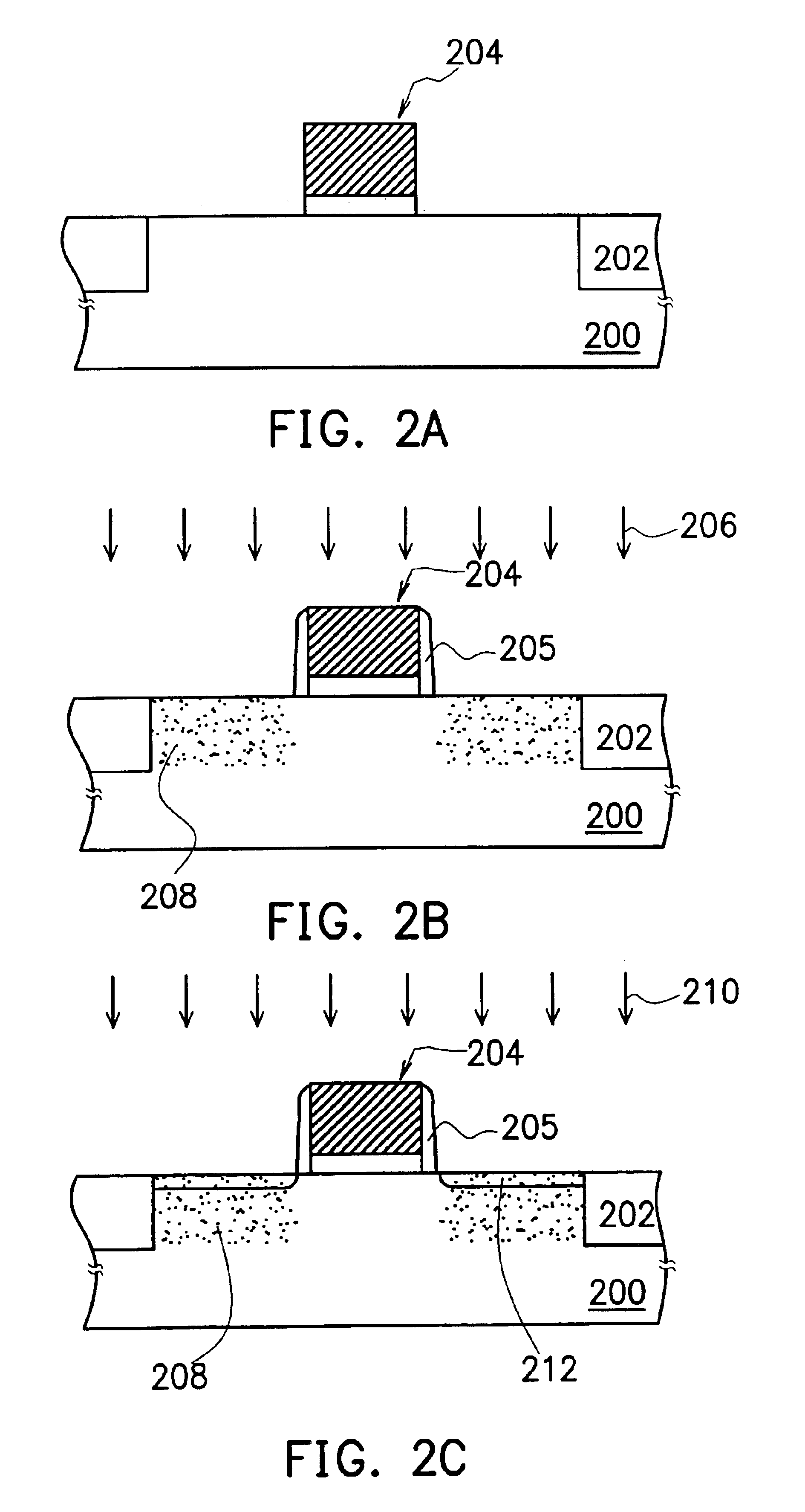
[0024]FIGS. 2A to 2E are schematic cross-sectional views showing the progression of steps for fabricating a metal-oxide-semiconductor transistor according to the preferred embodiment of this invention. First, as shown in FIG. 2A and step S102 of FIG. 1, a substrate 200 such as a silicon substrate with a shallow trench isolation region 202 therein and a gate structure 204 comprising a gate insulation layer and a gate thereon is formed over the substrate 200.

[0025]Thereafter, in step S104 of FIG. 1, a first spacer 205 is formed on the sidewalls...


PUM


Abstract

A method of manufacturing a MOS transistor is provided. A substrate having a gate structure thereon is provided. A first spacer is formed on the sidewall of the gate structure. A pre-amorphization implantation is carried out to amorphize a portion of the substrate. A doped source / drain extension region is formed in the substrate on each side of the first spacer. A second spacer is formed on the sidewall of the first spacer. A doped source / drain region is formed in the substrate on each side of the second spacer and then a pre-annealing operation is performed. Thereafter, a solid phase epitaxial process is carried out to re-crystallize the amorphized portion of the substrate and activate the doped source / drain extension region and the doped source / drain region to form a source / drain terminal. Finally, a post-annealing operation is performed.

Description

CROSS-REFERENCE TO RELATED APPLICATION[0001]This application claims the priority benefit of Taiwan application serial no. 92124424, filed on Sep. 4, 2003.BACKGROUND OF THE INVENTION[0002]1. Field of Invention[0003]The present invention relates to a method of manufacturing a semiconductor device. More particularly, the present invention relates to a method of manufacturing a metal-oxide-semiconductor (MOS) transistor.[0004]2. Description of Related Art[0005]As the level of integration in integrated circuits continues to increase, area occupation of each semiconductor device is reduced. Consequently, the specification in circuit design must be changed to reflect such reduction. At present, integrated circuits are designed to have feature dimensions in the deep sub-micron range. However, as the integrated circuit device such as a deep sub-micron metal-oxide-semiconductor (MOS) device is miniaturized, depth of the source / drain terminal within a substrate must be reduced in a correspondi...

Claims


Application Information

Patent Timeline
Patent Type & Authority Patents(United States)
IPC IPC(8): H01L21/265H01L21/02H01L21/336
CPCH01L21/26513H01L29/6656H01L29/6659H01L29/66666
Inventor WANG, YU-RENCHIEN, CHIN-CHENGWANG, HSIANG-YINGYANG, NENG-HUI
Owner UNITED MICROELECTRONICS CORP
Why Eureka
Try Eureka