Integrated camera and associated methods

Inactive Publication Date: 2008-06-12
FLIR SYSTEMS TRADING BELGIUM BVBA
View PDF75 Cites 44 Cited by
  • Summary
  • Abstract
  • Description
  • Claims
  • Application Information

AI Technical Summary

Benefits of technology

[0020]It is yet another feature of an embodiment to integrate optics wi

Problems solved by technology

Alignment accuracies of less than 15 microns for individual elements can be achieved using active alignment, but such accuracies greatly increase the amount of time spent moving the element.
Thus, such alignment accuracy is often impractical even using active alignment.
The alignment tolerance needed may be 1 micron to 5 microns, which is very expensive to achieve with conventional methods.
Unfortunately, these active alignment requirements are complex, time consuming, and relatively expensive.
Further, the level of size reduction in the vertical direction of an optical head is limited.
However, passive alignment has not been employed for wafer-to-wafer alignment.
In particular, the high density of solder bumps required and the thickness and mass of the wafer make such alignment impractical.
Another problem in integrating multiple optical elements formed on separate wafers at a wafer level arises due to the dicing process for forming the individual integrated elements.
The dicing process is messy due to the use of a dicing slurry.
However, when the wafers are bonded together, the slurry enters the gap between the wafers.
Removing the slurry from the gap formed between the wafers is quite diffi

Method used


Image

  • Integrated camera and associated methods
  • Integrated camera and associated methods
  • Integrated camera and associated methods

Examples


Embodiment Construction

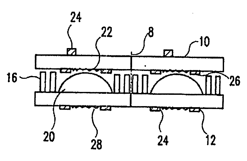
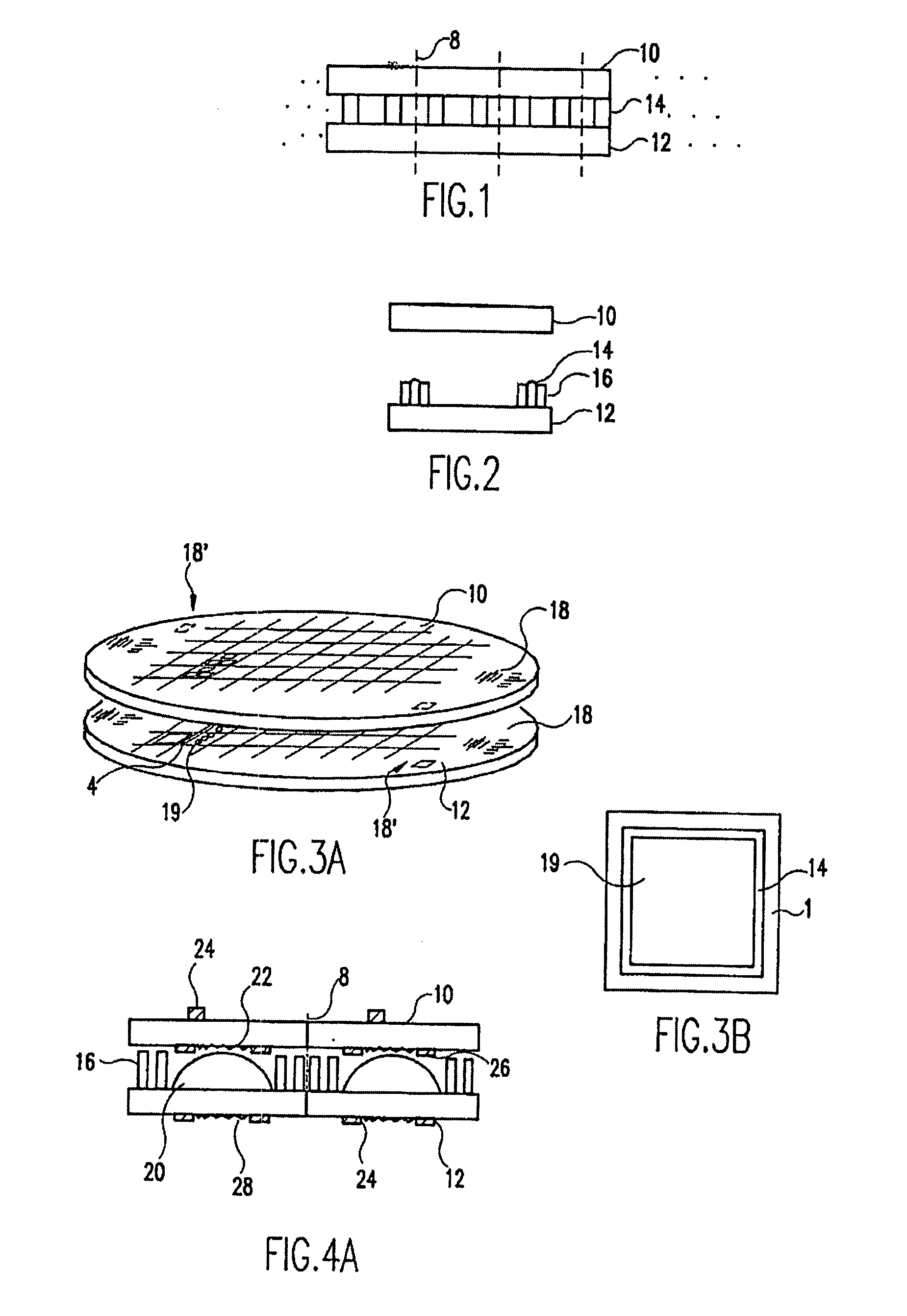
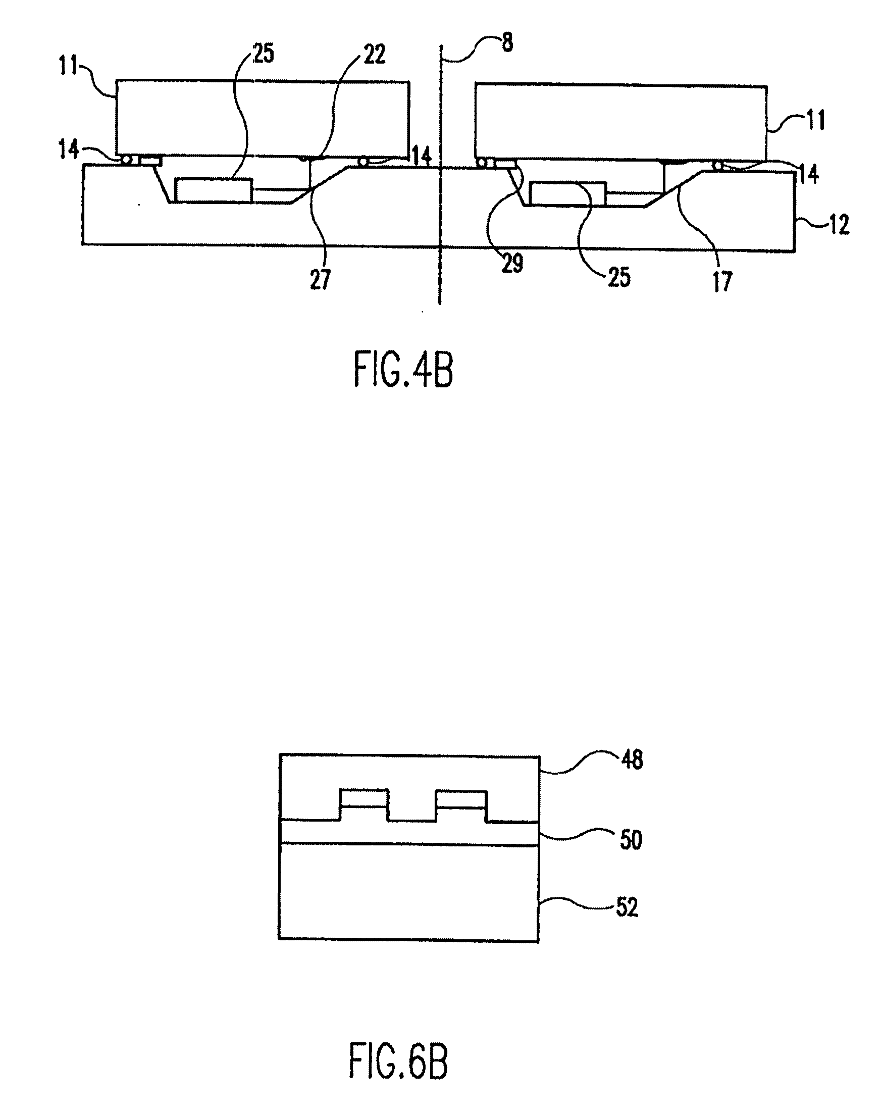
[0061]In the drawings, the thickness of layers and regions may be exaggerated for clarity. It will also be understood that when a layer is referred to as being “on” another layer or substrate, it may be directly on the other layer or substrate, or intervening layers may also be present. Further, it will be understood that when a layer is referred to as being “under” another layer, it may be directly under, or one or more intervening layers may also be present. In addition, it will also be understood that when a layer is referred to as being “between” two layers, it may be the only layer between the two layers, or one or more intervening layers may also be present. Like numbers refer to like elements throughout. As used herein, the term “wafer” is to mean any substrate on which a plurality of components are formed on a planar surface which are to be separated through the planar surface prior to final use.

[0062]As can be seen in FIG. 1, a first substrate wafer 10 and a second substrat...


PUM


Abstract

A method for forming a camera including an integrated optical subsystem, includes aligning a plurality of second dies with a plurality of first dies, each first die having a second die aligned therewith, at least one of the plurality of first dies and the plurality of the second dies include a corresponding number of optical elements, securing aligned dies, and dividing secured aligned dies into a plurality of portions, a portion containing a first die, a second die and at least one optical element, thereby forming the integrated optical subsystem.

Description

CROSS REFERENCES TO RELATED APPLICATIONS[0001]This application claims the benefit of priority under 35 U.S.C. §120 to U.S. application Ser. No. 08 / 727,837, filed Sep. 27, 1996 (now U.S. Pat. No. 5,771,218), Ser. No. 08 / 917,865, filed Aug. 27, 1997, (now U.S. Pat. No. 6,128,134), Ser. No. 08 / 943,274, filed Oct. 3, 1997 (now U.S. Pat. No. 6,096,155), Ser. No. 09 / 018,891, filed Feb. 5, 1998 (now U.S. Pat. No. 5,912,872), Ser. No. 09 / 503,249, filed Feb. 14, 2000 (now U.S. Pat. No. 6,610,166), Ser. No. 09 / 637,364, filed Aug. 15, 2000 (now U.S. Pat. No. 6,522,618), and pending Ser. No. 10 / 647,262, filed Aug. 26, 2003, which are hereby incorporated by reference in their entirety for all purposes.FIELD OF THE INVENTION[0002]The present invention is directed to integrating multiple optical elements on a wafer level. In particular, the present invention is directed to efficient creation of integrated multiple elements, and incorporation thereof into a camera.BACKGROUND OF THE INVENTION[0003]A...

Claims


Application Information

Patent Timeline
IPC IPC(8): H04N5/225
CPCG02B6/4214H01S5/005G02B6/4231G02B6/4232G02B6/4238G02B6/4239G02B6/43G02B2006/12102G02B2006/12107G11B7/1205G11B7/1353G11B7/1372G11B7/1374G11B7/22H01L25/167H01L27/14618H01L27/14625H01L27/14632H01L31/0232G02B6/4224H01L2924/0002G11B7/123H01L31/02325H01L31/02327H01L2924/00
Inventor KATHMAN, ALAN D.FELDMAN, MICHAEL R.HARDEN, BRIANWELCH, W. HUDSON
Owner FLIR SYSTEMS TRADING BELGIUM BVBA
Why Eureka
Try Eureka