Liquid crystal display device

Active Publication Date: 2008-06-12
PANASONIC LIQUID CRYSTAL DISPLAY CO LTD +1
View PDF3 Cites 123 Cited by
  • Summary
  • Abstract
  • Description
  • Claims
  • Application Information

AI Technical Summary

Benefits of technology

[0032]Typical advantageous effects obtained by the present invention are as follows.
[0033]According to the present invention, it is possible to provide a liquid crystal display device having a narrow p

Problems solved by technology

However, since the orientation film ORI1 is formed by coating, there arises a drawback that the orientation film ORI1 spreads to the outside of the display region AR.
However, along with narrowing of

Method used


Image

  • Liquid crystal display device
  • Liquid crystal display device
  • Liquid crystal display device

Examples


embodiment 1

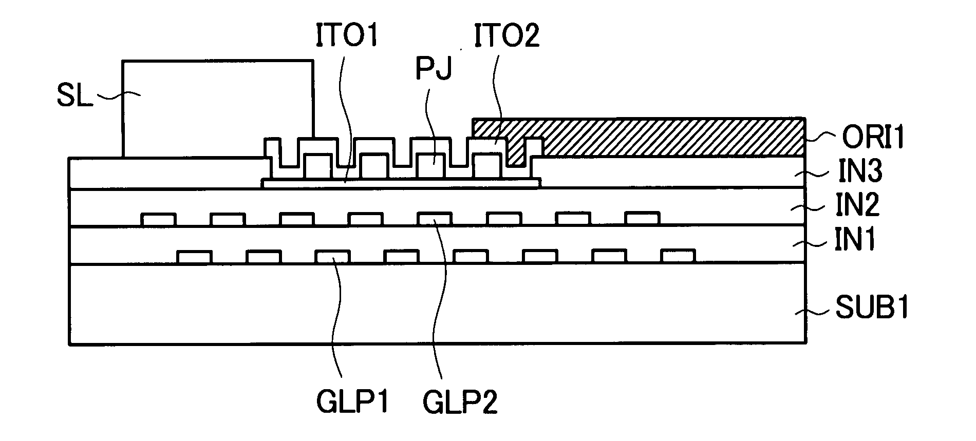
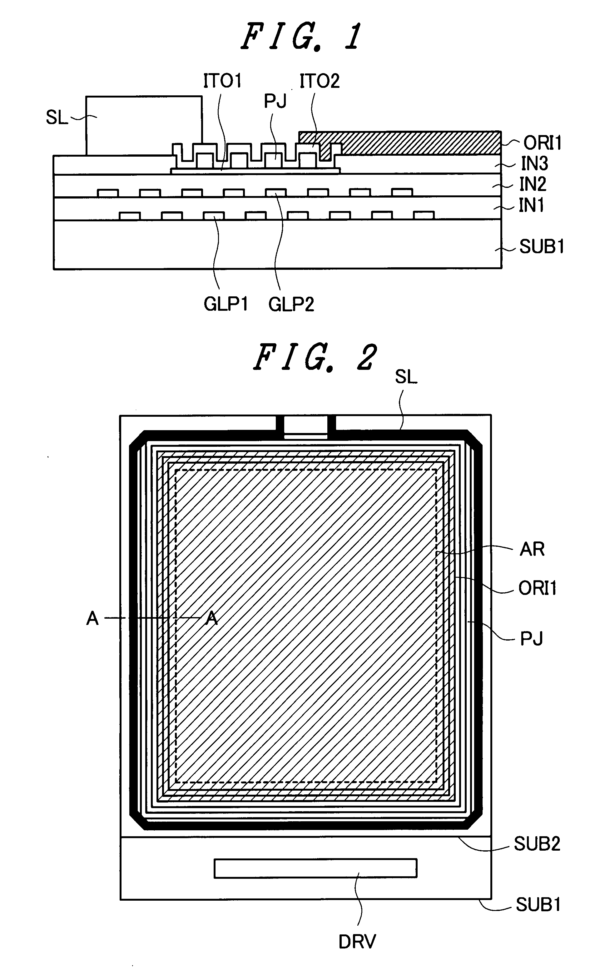
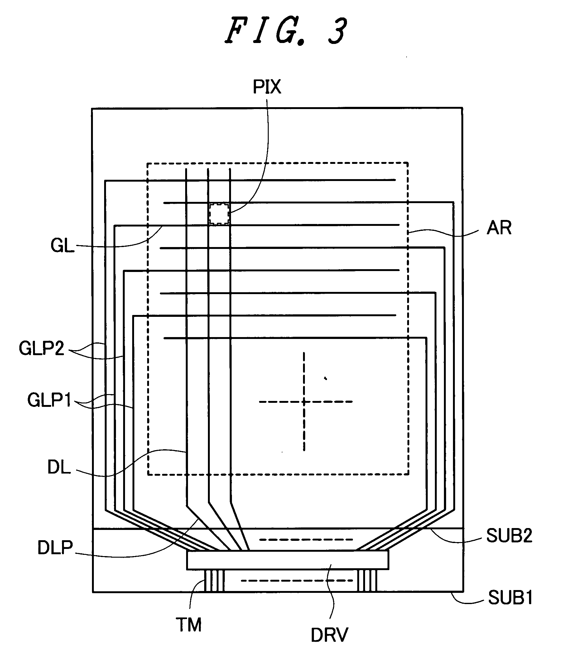
[0052]FIG. 1 is a view for explaining a liquid crystal display device of an embodiment 1 according to the present invention, and also is a cross-sectional view taken along a line A-A in FIG. 2. FIG. 2 is a plan view for explaining the liquid crystal display device of the embodiment 1 according to the present invention. FIG. 3 is a plan view for explaining one example of a layout of wiring of the embodiment 1 according to the present invention. FIG. 4 is a plan view for explaining an equivalent circuit of a pixel.

[0053]As shown in FIG. 2, the liquid crystal display device of this embodiment is configured such that liquid crystal LC not shown in the drawing is sandwiched between a transparent insulating substrate (first substrate) SUB1 made of glass or the like and a transparent insulating counter substrate (second substrate) SUB2 made of glass or the like. Here, the substrate SUB1 and the counter substrate SUB2 are adhered to each other using a sealing material SL. The liquid crystal...

embodiment 2

[0067]Next, the present invention is explained in conjunction with a case in which the present invention is applied to an IPS-type liquid crystal display device. FIG. 5 is a plan view of one example of the pixel for explaining the liquid crystal display device of an embodiment 2 according to the present invention. FIG. 6 is a cross-sectional view taken along a line B-B in FIG. 5.

[0068]As shown in FIG. 5 and FIG. 6, portions of the scanning signal lines GL which are formed on the substrate SUB1 constitute the gate electrodes GT of the thin film transistors TFT. Here, the scanning-signal-line lead lines GLP1 explained in the embodiment 1 are also simultaneously formed. The insulation film IN1 explained in the embodiment 1 is formed on the scanning-signal-line lead lines GLP1 and functions as a gate insulation film. Semiconductor films AS made of amorphous silicon or the like, for example, are formed on the insulation film IN1. On the semiconductor films AS, the video signal lines DL, ...

embodiment 3

[0072]Next, the present invention is explained in conjunction with a case in which the present invention is applied to a liquid crystal display device of a vertical electrical field type. FIG. 7 is a plan view of one example of the pixel for explaining the liquid crystal display device of an embodiment 3 according to the present invention. FIG. 8 is a cross-sectional view taken along a line C-C in FIG. 7. Here, in the embodiment 3, the explanation is made only with respect to the constitution which makes this embodiment differ from the embodiment 2, and the explanation of parts identical with the parts in the embodiments 1, 2 is omitted.

[0073]As shown in FIG. 7 and FIG. 8, in the embodiment 3, the counter electrode CT is formed on the counter-substrate-SUB2 side, for example, between the orientation film ORI2 and the overcoat film OC. Further, the pixel electrode PX is formed on the substantially whole area of the pixel region PIX in a planar shape. Further, the liquid crystal LC is...


PUM


Abstract

The present invention provides a liquid crystal display device with a narrow picture frame which reduces a sealing defect by suppressing spreading of an orientation film. In a region inside a sealing material and outside a display region, an uneven surface for suppressing spreading of the orientation film is formed. It is preferable that the uneven surface is formed using an insulation film and, at the same time, an etching stopper layer is formed below the insulation film which forms the uneven surface. It is more preferable that the uneven surface and the stopper layer are simultaneously formed with a layer used for forming pixels in a step for forming such a layer thus preventing the increase of manufacturing steps.

Description

[0001]The present application claims priority from Japanese application JP2006-328939 filed on Dec. 6, 2006, the content of which is hereby incorporated by reference into this application.BACKGROUND OF THE INVENTION[0002]1. Field of the Invention[0003]The present invention relates to a liquid crystal display device, and more particularly to a technique which is effectively applicable to a liquid crystal display device with a narrow picture frame region.[0004]2. Description of the Related Art[0005]A liquid crystal display device has been used as display devices of various sizes used in applications ranging from a miniaturized mobile phone to a large-sized television receiver set.[0006]FIG. 16 is a plan view for explaining a conventional liquid crystal display device. Here, a miniaturized liquid crystal display device is illustrated as one example. In the liquid crystal display device, a substrate SUB1 and a counter substrate SUB2 are adhered to each other using a sealing material SL,...

Claims


Application Information

Patent Timeline
IPC IPC(8): G02F1/1339
CPCG02F1/1337G02F2001/13415G02F1/1341G02F1/1339G02F1/13415
Inventor KOMENO, HITOSHIKOSHITA, TOSHIYUKI
Owner PANASONIC LIQUID CRYSTAL DISPLAY CO LTD
Why Eureka
Try Eureka