Leadframe on heat sink (LOHS) semiconductor packages and fabrication methods thereof

Active Publication Date: 2008-06-19
MEDIATEK INC
View PDF11 Cites 127 Cited by
  • Summary
  • Abstract
  • Description
  • Claims
  • Application Information

AI Technical Summary

Benefits of technology

[0016]The invention relates to integration of leadframe on heat sink (LOHS) with multi-chips (system) mounted in a package (SiP). Mean

Problems solved by technology

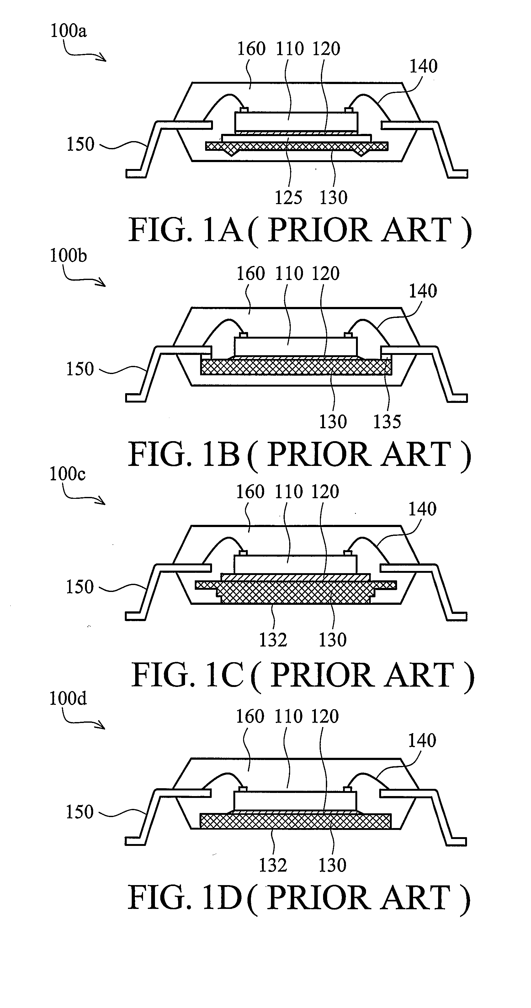
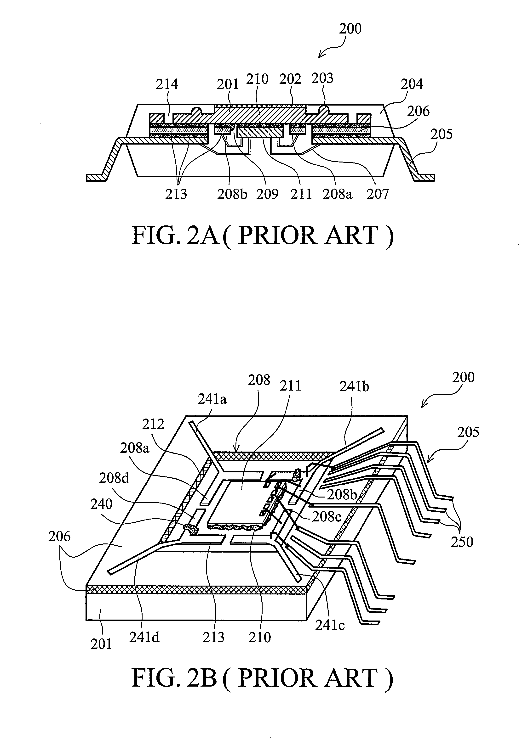
Two main semiconductor packaging challenges encountered with high-speed data transmissions are: 1) thermal problems due to greater power consumption requirements; and 2) electrical problems due to higher signal bandwidth.
However, letting the heat sink act as a ground plane or floating ground plane does not improve the electrical performance effectively.
However, the problem, of this type des

Method used


Image

  • Leadframe on heat sink (LOHS) semiconductor packages and fabrication methods thereof
  • Leadframe on heat sink (LOHS) semiconductor packages and fabrication methods thereof
  • Leadframe on heat sink (LOHS) semiconductor packages and fabrication methods thereof

Examples


Example

[0035]It is to be understood that the following disclosure provides many different embodiments, or examples, for implementing different features of various embodiments. Specific examples of components and arrangements are described below to simplify the present disclosure. These are merely examples and are not intended to be limiting. In addition, the present disclosure may repeat reference numerals and / or letters in the various examples. This repetition is for the purpose of simplicity and clarity and does not in itself indicate a relationship between the various embodiments and / or configurations discussed. Moreover, the formation of a first feature over or on a second feature in the description that follows may include embodiments in which the first and second features are formed in direct contact or not in direct contact.

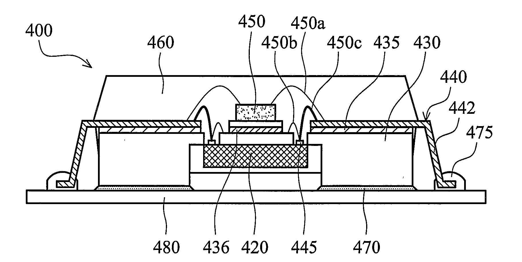
[0036]FIG. 4A is a cross section of an embodiment of a lead on heat sink (LOHS) system in package (SiP) of the invention. FIG. 4B is a plan view of the LOHS-SiP ...


PUM


Abstract

The invention relates to leadframe semiconductor packages mounted on a heat-sink and fabrication thereof. A system in package (SiP) comprises a leadframe having extension leads, configured with divisional heat sinks serving as power and ground nets. A set of semiconductor dies is attached by adhesive on the central region of the lead frame. Pluralities of wire bonds electrically connect the set of semiconductor dies to the leadframe and to the divisional heat sinks respectively. An encapsulation encloses the leadframe, but leaves the extension leads and the divisional heat sink uncovered, exposing a heat dissipating surface.

Description

CROSS-REFERENCE TO RELATED APPLICATIONS[0001]This application claims the benefit of U.S. Provisional Application No. 60 / 870,445 filed on Dec. 18, 2006, the entirety of which is incorporated herein by reference.BACKGROUND OF THE INVENTION[0002]1. Field of the Invention[0003]The invention relates to semiconductor packages, and in particular, to leadframe semiconductor packages mounted on a heat-sink and fabrication thereof.[0004]2. Description of the Related Art[0005]Requirements for faster signal transmissions are being driven by consumer demand for electronic devices with greater bandwidth capacity. Two main semiconductor packaging challenges encountered with high-speed data transmissions are: 1) thermal problems due to greater power consumption requirements; and 2) electrical problems due to higher signal bandwidth. In order to solve signal and power integrity (F3dB=0.35 / tr) and heat dissipation (P=CL×f×VDD2) issues, semiconductor packaging with both lower parasitic effects and low...

Claims


Application Information

Patent Timeline
IPC IPC(8): H01L23/36
CPCH01L2924/014H01L2924/01023H01L2924/01074H01L23/3107H01L23/4334H01L23/49541H01L23/49575H01L23/49589H01L24/49H01L2224/32245H01L2224/48091H01L2224/4824H01L2224/48247H01L2224/4826H01L2224/49109H01L2224/4911H01L2224/73215H01L2224/73265H01L2924/01013H01L2924/01028H01L2924/01029H01L2924/01033H01L2924/01046H01L2924/01047H01L2924/01078H01L2924/01079H01L2924/01082H01L2924/14H01L2924/1433H01L2924/19041H01L2924/30107H01L2924/3011H01L2924/3025H01L2924/01087H01L2924/01006H01L24/48H01L2924/00014H01L2924/00H01L2924/181H01L2924/351H01L2224/45099H01L2224/05599H01L2924/00012
Inventor CHEN, NAN-JANGLIN, HONG-CHIN
Owner MEDIATEK INC
Why Eureka
Try Eureka