Stacked package and method for manufacturing the package

Active Publication Date: 2008-06-19
SHINKO ELECTRIC IND CO LTD
View PDF7 Cites 22 Cited by
  • Summary
  • Abstract
  • Description
  • Claims
  • Application Information

AI Technical Summary

Benefits of technology

[0022]According to the present invention, the connection sections which stack a plurality of packages one on top of the other in an electrically connected manner are structured by comprising pillar-like members for supporting a substrate which is to serve as an upper layer on a substrate which is to serve as a lower layer, whereby a pitch between the adjace

Problems solved by technology

However, processing for inserting the underfill resin is troublesome, whic

Method used


Image

  • Stacked package and method for manufacturing the package
  • Stacked package and method for manufacturing the package
  • Stacked package and method for manufacturing the package

Examples


Example

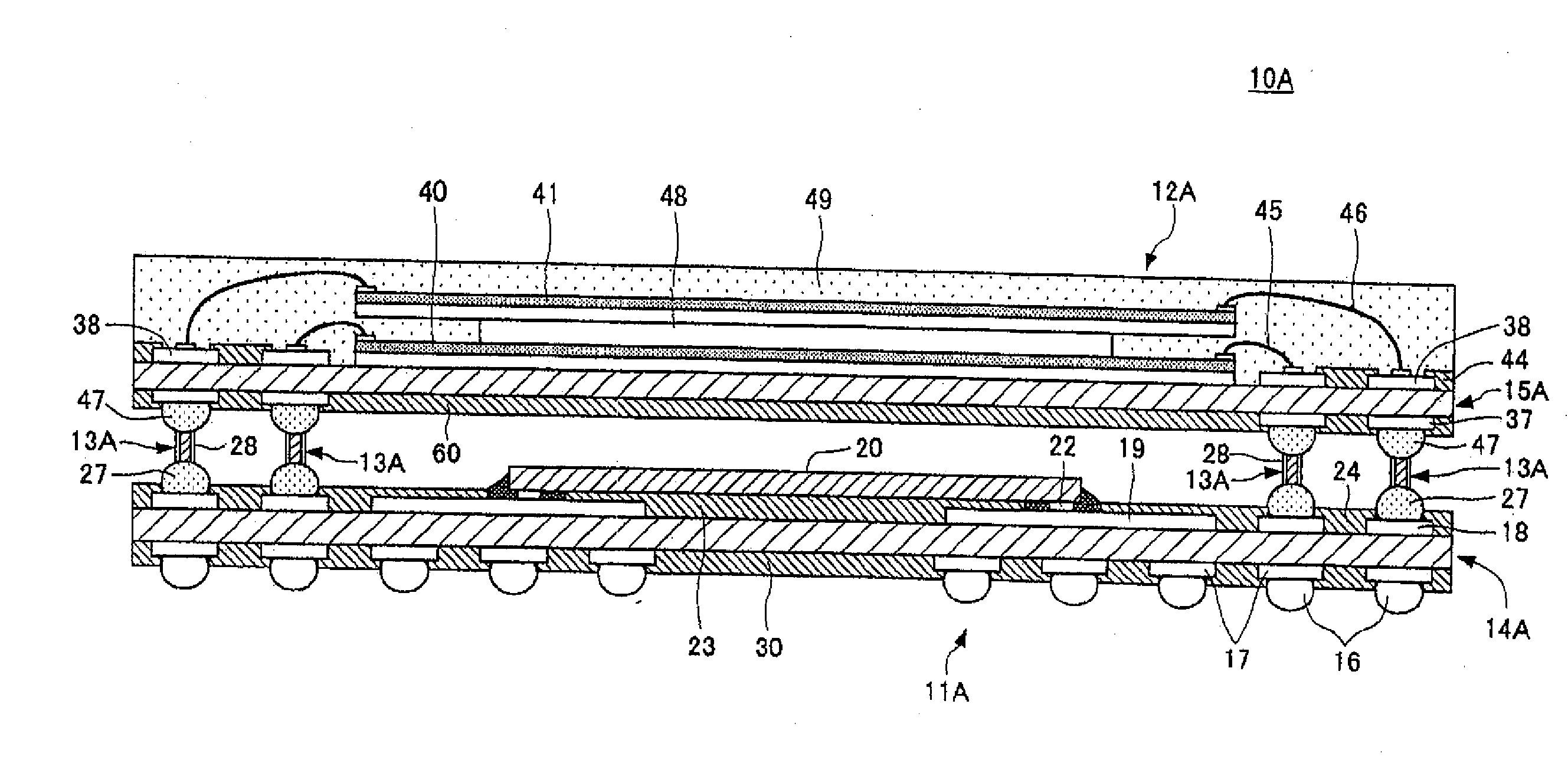
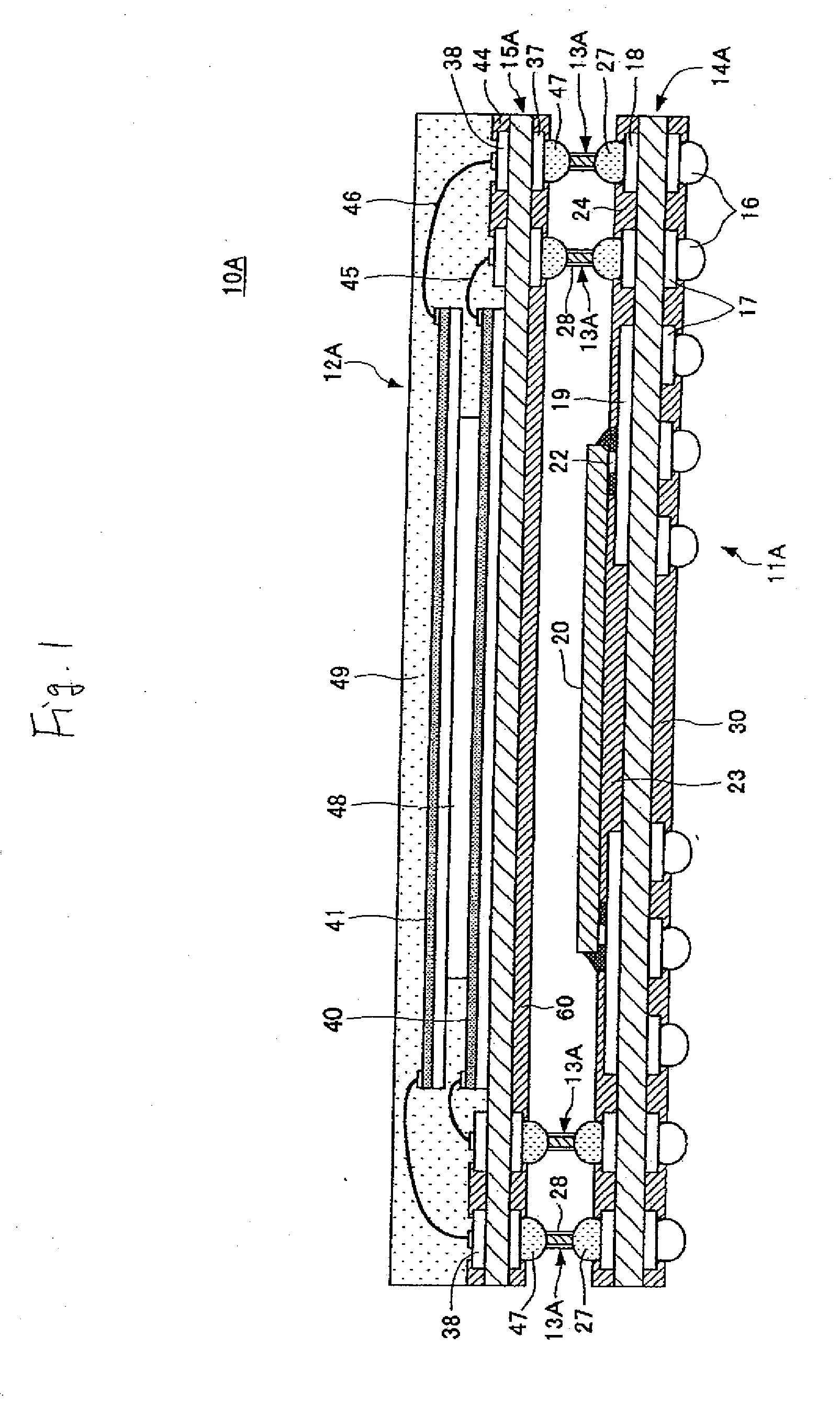
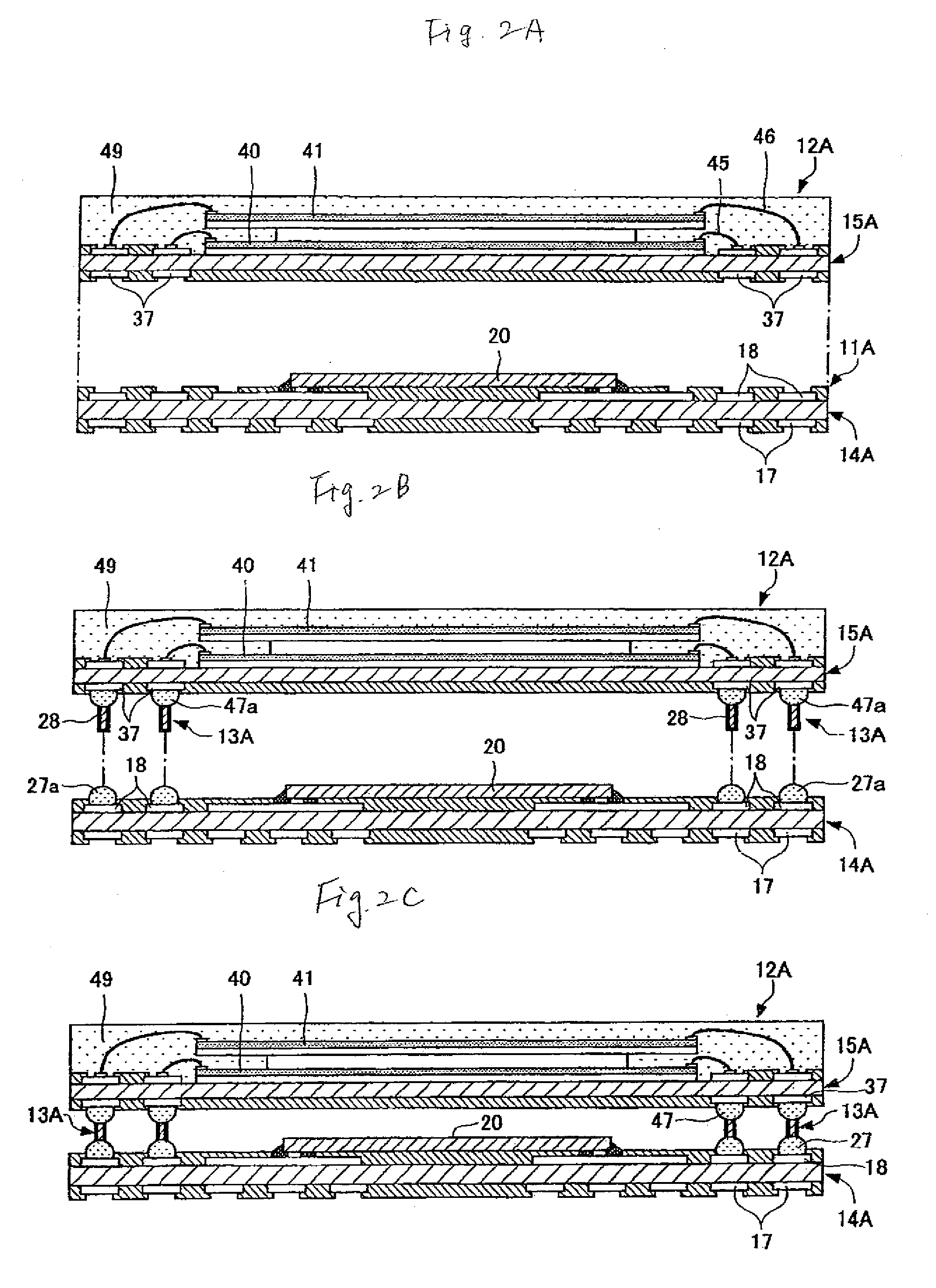
[0032]FIG. 1 shows a stacked package 10A according to a first embodiment of the present invention. The stacked package 10A shown in the drawing comprises a lower package 11A, an upper package 12A, and connection sections.

[0033]The lower package 11A is formed from a lower substrate 14A, solder balls 16, lower electrodes 17, upper electrodes 18, a semiconductor element 20, and the like. The lower substrate 14A is a resin substrate and configured in such a way that a conductor film (e.g., a Cu film) is formed on upper and lower surfaces of a substrate main body formed from an insulating resin by plating or the like.

[0034]The conductor film is subject to a predetermined patterning by etching and the like, whereby wiring lines are formed on the upper and lower surfaces of the substrate main body. Portions of lower wiring lines (not shown) formed on the lower surface of the substrate main body constitute the lower electrodes 17, and portions of upper wiring lines 19 formed on the upper su...

Example

[0061]The stacked package 10B of the second embodiment shown in FIG. 3 is characterized in that a plurality of semiconductor elements 20 and 21 (two in the present embodiment) are stacked on a lower package 11B.

[0062]The lower package 11B is structured in such a way that the semiconductor element 20 and the semiconductor element 21 are stacked on an upper surface of a lower substrate 14B by way of a spacer 31. Further, the respective semiconductor elements 20, 21 are electrically connected to the lower substrate 14B by wires 25 and 26.

[0063]A sealing resin 50 is formed so as to seal the respective semiconductor elements 20 and 21 and the wires 25 and 26. A range where the sealing resin 50 is formed is limited to areas where the respective semiconductor elements 20 and 21 and the wires 25 and 26 are formed. Upper electrodes 18 where pillar-like members 13B are to be provided are formed so as to become exposed through the solder resist.

[0064]In the meantime, in the present embodiment,...

Example

[0070]FIG. 5 shows the stacked package 10C of the third embodiment. The stacked package 10C is characterized in that at least either upper or lower ends of respective pillar-like members 13C constituting the connection sections are inserted into insertion holes formed in an upper or lower substrate.

[0071]In the present embodiment, upper ends of the pillar-like members 13C are bonded to lower electrodes 37 of an upper package 12C (an upper substrate 15C) by use of solder joint sections 47, and lower ends of the pillar-like members 13C are inserted into the insertion holes 29 formed in a lower package 11C (a lower substrate 14C).

[0072]Electrodes 55 are formed in the respective insertion holes 29 of the lower substrate 14C, and the pillar-like members 13C are inserted into the respective insertion holes 29, to thus become electrically connected to the electrodes 55. The electrodes 55 may also be formed by through holes or vias, or contact components may also be provided separately.

[007...


PUM


Abstract

In a stacked package in which a plurality of packages having semiconductor elements mounted on substrates are stacked, while being electrically connected together, by use of connection sections, wherein the connection sections are formed from pillar-like members and solder joint sections and the upper package is supported on the lower package by pillar-like members.

Description

[0001]This application claims priority to Japanese Patent Application No. 2006-336276, filed Dec. 13, 2006, in the Japanese Patent Office. The priority application is incorporated by reference in its entirety.TECHNICAL FIELD[0002]The present disclosure relates to a stacked package and a method of manufacturing the package. More particularly, the present disclosure relates to a stacked package for which a plurality of packages are stacked while being electrically connected together by use of connection sections, and a method for manufacturing the package.RELATED ART[0003]A module product called a system-in-package realized by packing a plurality of semiconductor elements or passive components into a single package has recently been commercialized as described in; e.g., Patent Document 1. FIG. 7 shows a system-in-package 100 according to an example of the related art.[0004]The system-in-package 100 shown in the drawing has a structure in which an upper package 112 is stacked on a lowe...

Claims


Application Information

Patent Timeline
IPC IPC(8): H01L23/538H01L21/58
CPCH01L25/105H01L2225/1058H01L2224/48227H01L2224/73265H01L2224/83102H01L2224/92125H01L2225/0651H01L2225/06575H01L2924/01004H01L2924/01078H01L2924/01079H01L2924/15311H01L2924/15331H05K3/3436H05K3/3447H05K2201/10242H05K2201/10303H05K2201/10318H05K2201/10719H05K2201/10946H01L2224/48091H01L2225/1023H01L2224/73204H01L2224/32225H01L2224/32145H01L2224/16225H01L2924/00014H01L2924/00H01L2924/00012H01L24/73H01L2924/14H01L2924/00011Y02P70/50H01L2224/0401H01L23/12
Inventor OI, KIYOSHICHINO, TERUAKI
Owner SHINKO ELECTRIC IND CO LTD
Why Eureka
Try Eureka