Semiconductor integrated circuit and manufacturing method therefor

a technology of integrated circuits and semiconductors, applied in pulse generators, pulse techniques, instruments, etc., can solve the problems of low manufacturing yield of mos lsi, remarkably high operation power consumption, and complex control, and achieve low overhead, high manufacturing yield, and small size

Inactive Publication Date: 2008-06-19
RENESAS ELECTRONICS CORP
View PDF8 Cites 42 Cited by
  • Summary
  • Abstract
  • Description
  • Claims
  • Application Information

AI Technical Summary

Benefits of technology

[0013]In a representative semiconductor integrated circuit of the present invention, an active body bias technique is employed. In the active body bias technique, a body bias voltage is applied to the substrate of a MOS transistor in an active mode in which the semiconductor integrated circuit processes an input signal. In the active body bias technique, first, a threshold voltage of the MOS transistor is measured. If the threshold voltage varies largely, the level of the body bias voltage is adjusted to control the variations to a predetermined error range. To the substrate (well) of the MOS transistor, a body bias voltage of a reverse bod

Problems solved by technology

Specifically, when the threshold voltage of the MOS transistor is too low, the operation power consumption increases remarkably in the active mode in which the semiconductor integrated circuit performs processes on a digital input signal and an analog digital signal.
As a result, the process window of the threshold voltage of the MOS transistor at the ti

Method used


Image

  • Semiconductor integrated circuit and manufacturing method therefor
  • Semiconductor integrated circuit and manufacturing method therefor
  • Semiconductor integrated circuit and manufacturing method therefor

Examples


Embodiment Construction

Representative Embodiments

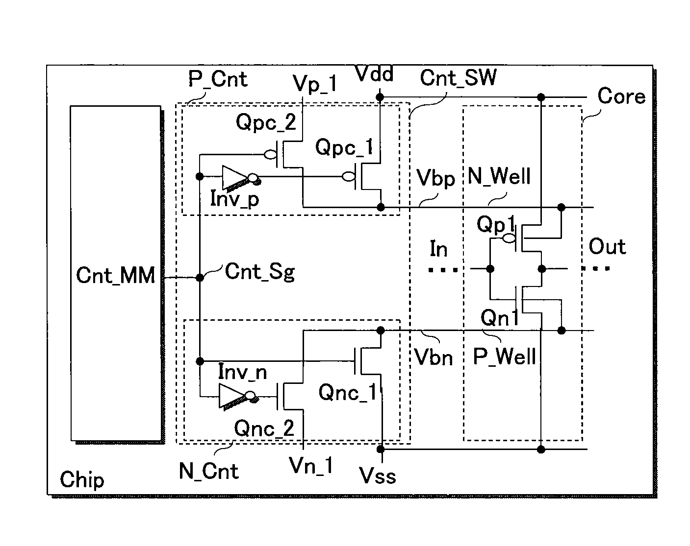
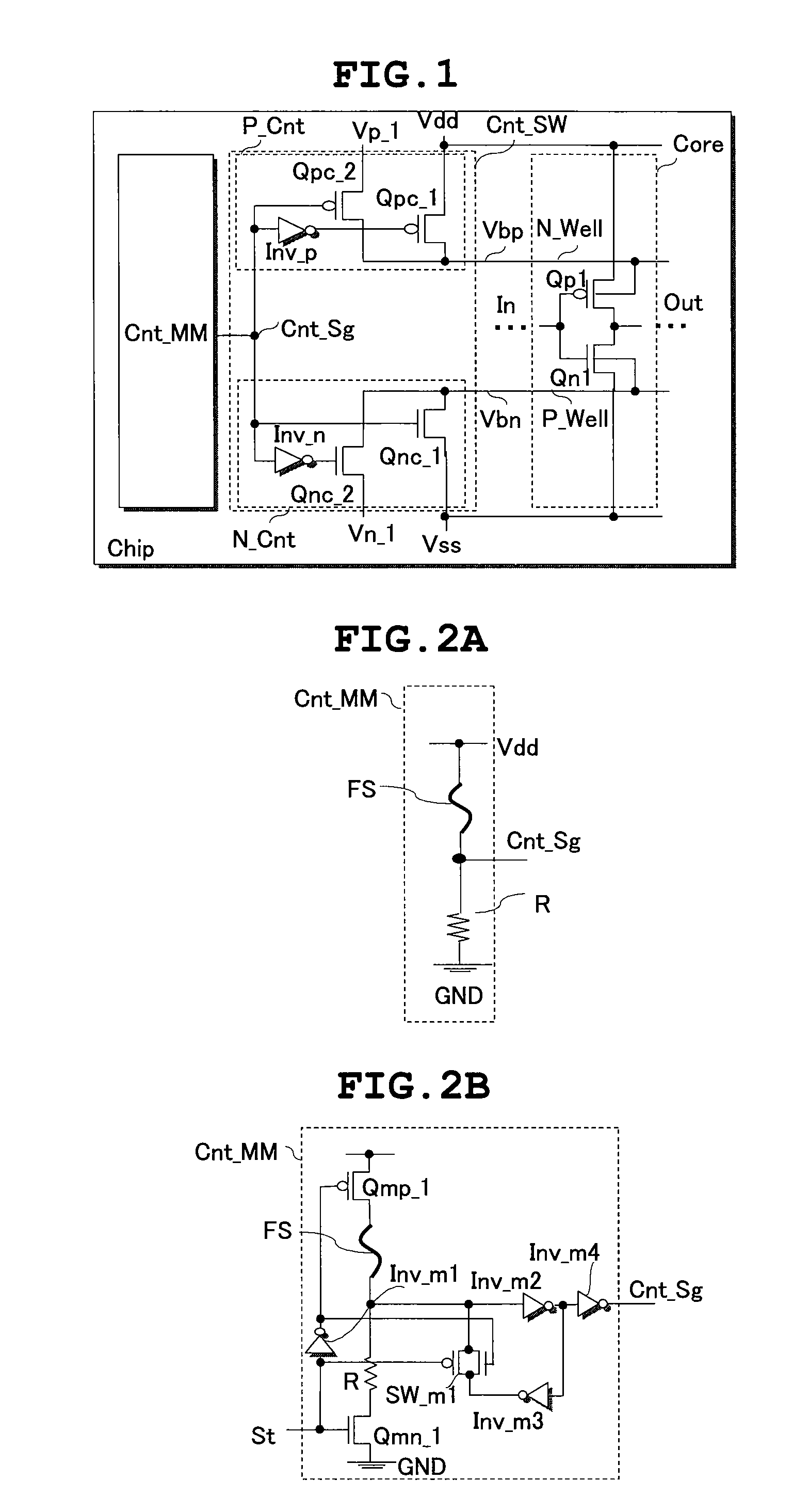
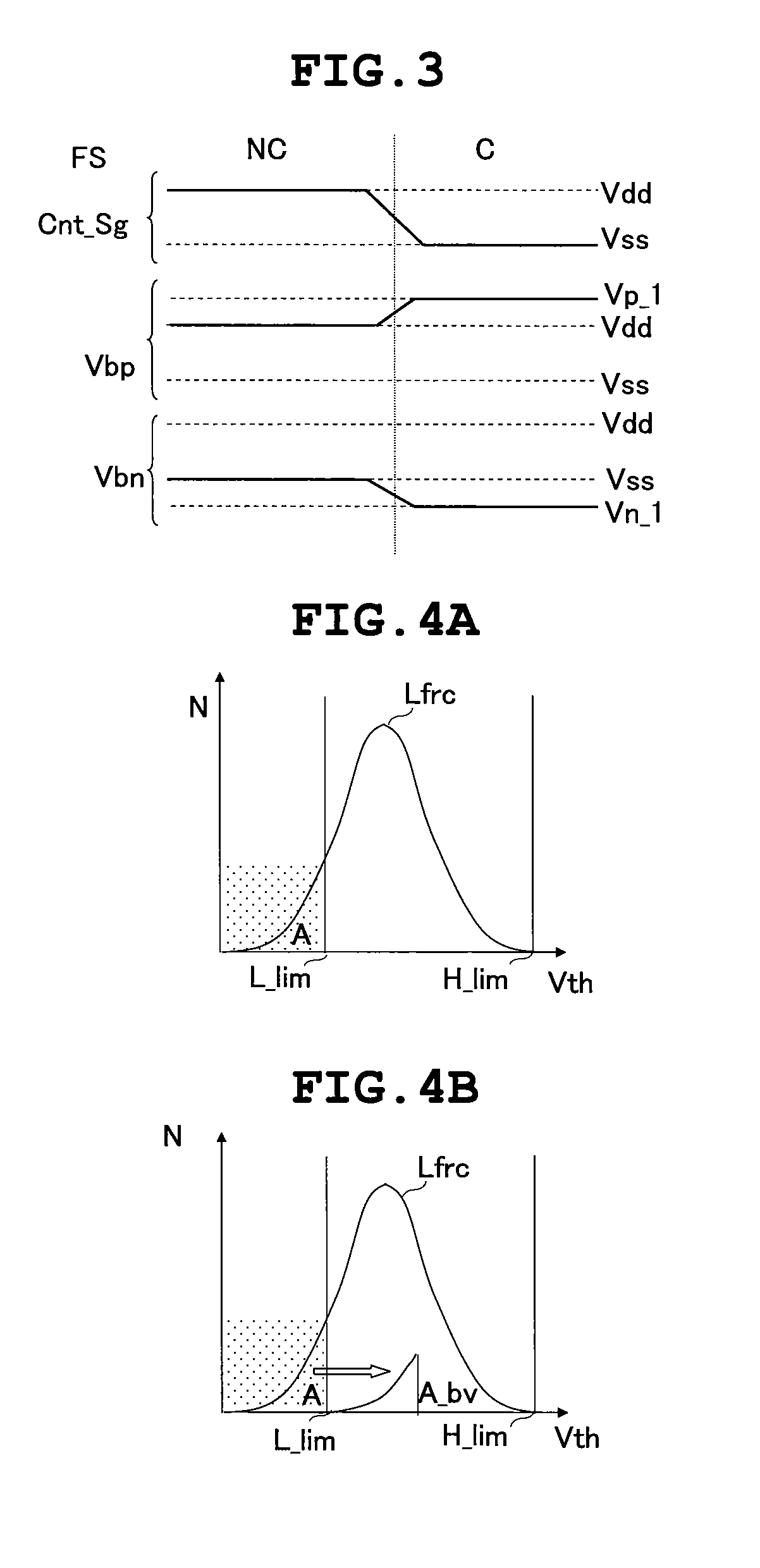
[0048]First, outline of representative embodiments of the present invention disclosed in the application will be described. Reference numerals in the drawings described in parenthesis in the representative embodiments just illustrate parts included in the concept of the components.[0049][1] A semiconductor integrated circuit (Chip) as a representative embodiment of the present invention includes a CMOS circuit (Core) for processing an input signal (In) in an active mode. The semiconductor integrated circuit further includes a control switch (Cnt_SW) for supplying a pMOS body bias voltage (Vbp) and an nMOS body bias voltage (Vbn) to an N well (N_Well) in a pMOS transistor (Qp1) and a P well (P_Well) in an nMOS transistor (Qn1), respectively, in the CMOS circuit. The semiconductor integrated circuit further includes a control memory (Cnt_MM) for storing at least control information (Cnt_Sg) indicating whether or not the pMOS body bias voltage and the nMOS bod...


PUM


Abstract

The present invention is directed to realize high manufacture yield and compensate variations in threshold voltage of a MOS transistor with small overhead. A semiconductor integrated circuit includes a CMOS circuit for processing an input signal in an active mode, a control switch, and a control memory. The control switch supplies a pMOS body bias voltage and an nMOS body bias voltage to an N well in a pMOS transistor and a P well in an nMOS transistor, respectively, in the CMOS circuit. The control memory stores control information indicating whether or not the pMOS body bias voltage and the nMOS body bias voltage are supplied from the control switch to the N well in the pMOS transistor and the P well in the nMOS transistor, respectively, in the CMOS circuit in the active mode.

Description

CLAIM OF PRIORITY[0001]The present application claims priority from Japanese application JP2006-339437 filed on Dec. 18, 2006, the content of which is hereby incorporated by reference into this application.FIELD OF THE INVENTION[0002]The present invention relates to a semiconductor integrated circuit and a method of manufacturing the same. More particularly, the invention relates to the technique useful for realizing higher manufacture yield and compensating variations in threshold voltage of a MOS transistor with small overhead.BACKGROUND OF THE INVENTION[0003]Due to the short channel effect produced as a semiconductor device is becoming finer, the threshold voltage of a MOS transistor is decreasing and increase in the subthreshold leakage current is becoming apparent. The characteristic equal to or less than the threshold voltage of the MOS transistor is the subthreshold characteristic, and leakage current in a state where the surface of MOS silicon is weakly inverted is called su...

Claims


Application Information

Patent Timeline
IPC IPC(8): H03K3/01H01L21/8238
CPCH01L21/823878H01L21/823892H03K19/00315H01L27/1203H03K19/0027H01L27/092G11C5/14G11C7/08
Inventor KOMATSU, SHIGENOBUOSADA, KENICHIYAMAOKA, MASANAOISHIBASHI, KOICHIRO
Owner RENESAS ELECTRONICS CORP
Why Eureka
Try Eureka