
Eureka
For R&D, Eureka makes reading and utilizing patents & technical documents easy.
Eureka AIR
Designed for self-driven R&D workflows. Generate viable solutions, solve complex R&D challenges, empower your innovation with AI.

Eureka Materials
Designed for material experts only. Revolutionize your material R&D, from search, analyze, to developing new materials.

TechResearch
Generate reliable direction feasibility study reports for your R&D in just a few steps.

TechSeek
Discover and master advanced knowledge NOW. Basics, ideas, possibilities, all at once.

TechMind
As an expert in R&D Theories, TechMind can generates customized viable solutions instantly.

TechRisk
Analyze your overall solution with one click, know your potential R&D risks in advance.

TechMonitor
Get weekly tech updates, stay abreast of the latest tech innovations and key insights.
Position measurement apparatus, imaging apparatus, exposure apparatus, and device manufacturing method
- Summary
- Abstract
- Description
- Claims
- Application Information
AI Technical Summary
Benefits of technology
Problems solved by technology
Method used
Image

Examples
first exemplary embodiment
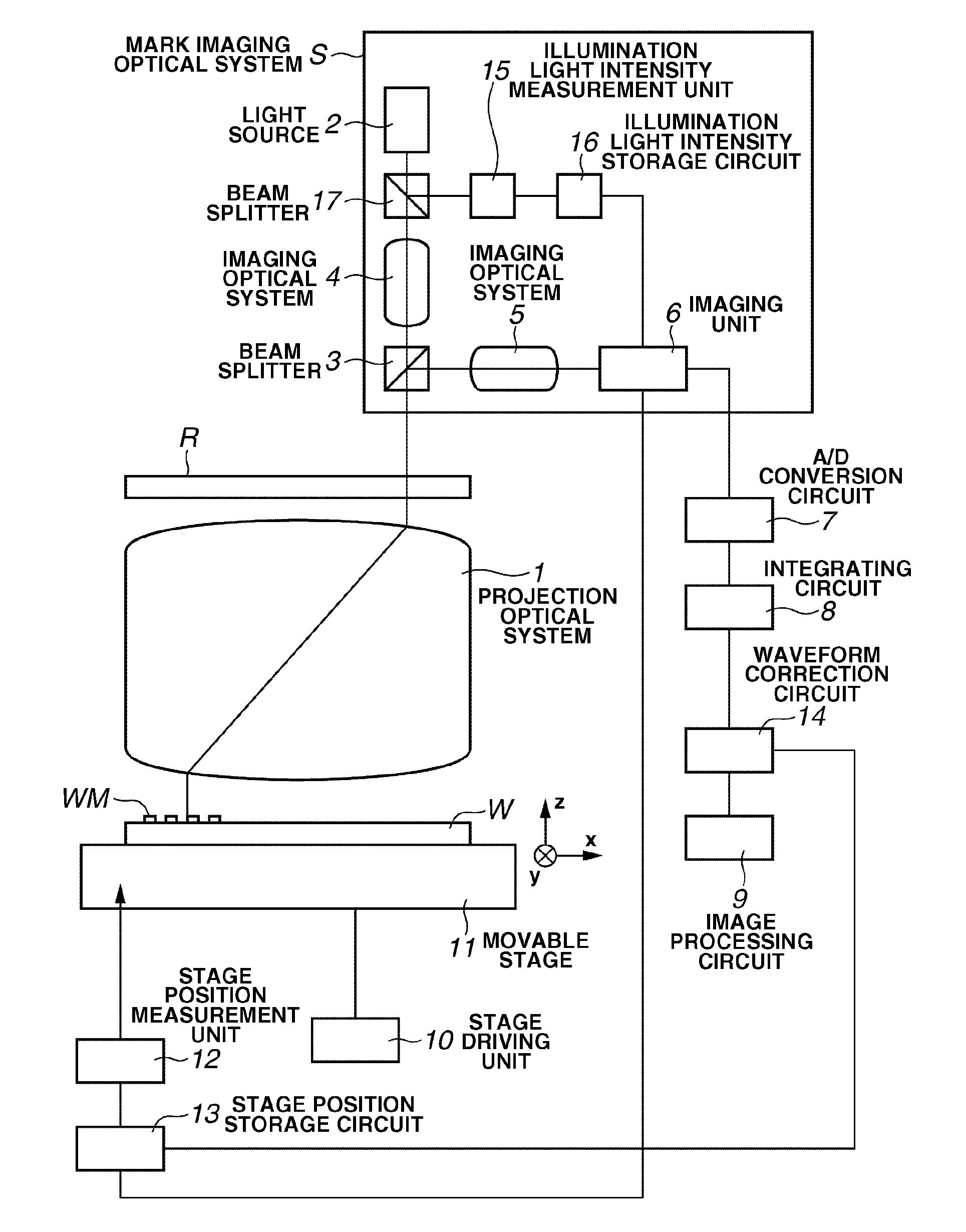
[0030]FIG. 1 illustrates an exposure apparatus capable of manufacturing semiconductor devices according to a first exemplary embodiment of the present invention. In FIG. 1, “R” represents a reticle, “W” represents a wafer (i.e., a substrate to be exposed), and “WM” represents a wafer mark. A projection optical system 1 has an optical axis parallel to a z-axis of the xyz-coordinate system. A mark imaging optical system S includes a light source 2, two beam splitters 3 and 17, two imaging optical systems 4 and 5, an imaging unit 6 (e.g., CCD), an illumination light intensity measurement unit 15 measuring an intensity of light emitted toward the wafer mark WM, and an illumination light intensity storage circuit 16.
[0031]An analog / digital (A / D) conversion circuit 7 receives an analog image signal from the mark imaging optical system S and converts the input analog signal into a digital signal. An integrating circuit 8 generates a one-dimensional digital signal sequence. An image process...
second exemplary embodiment
[0049]According to the first exemplary embodiment, the stage driving unit 10 moves the stage 11 to a position where the position measurement unit 12 can observe the wafer mark WM on the stage 11 and stops the stage 11 to execute a mark position measurement. A second exemplary embodiment is different from the first exemplary embodiment in performing the mark position measurement when the stage 11 is moving.
[0050]The exposure apparatus according to the second exemplary embodiment has a hardware arrangement similar to that of the first exemplary embodiment and is not described below. First, the stage driving unit 10 moves the stage 11. The position measurement unit 12 starts the mark position measurement after the wafer mark WM on the stage 11 enters an observation range of the imaging unit 6. The mark position measurement includes emitting a luminous flux from the light source 2 and illuminating the wafer mark WM via the beam splitters 17 and 3, the imaging optical system 4, the retic...
third exemplary embodiment
[0059]FIG. 6 illustrates an exposure apparatus capable of manufacturing semiconductor devices according to a third exemplary embodiment of the present invention. In FIG. 6, “R” represents a reticle, “W” represents a wafer (i.e., a substrate to be exposed), and “WM” represents a wafer mark. A projection optical system 1 has an optical axis parallel to a z-axis of the xyz-coordinate system. A mark imaging optical system S includes a light source 2, two beam splitters 3 and 17, two imaging optical systems 4 and 5, an imaging unit 6 (e.g., CCD), an illumination light intensity measurement unit 15 measuring an intensity of light emitted toward the wafer mark WM, and an illumination light intensity storage circuit (unit) 16.
[0060]An analog / digital (A / D) conversion circuit 7 receives an analog image signal from the mark imaging optical system S and converts the input analog signal into a digital signal. An integrating circuit 8 generates a one-dimensional digital signal sequence. An image ...
PUM
 Abstract
Description
Claims
Application Information
 - R&D Engineer
- R&D Manager
- IP Professional
- Industry Leading Data Capabilities
- Powerful AI technology
- Patent DNA Extraction
Browse by: Latest US Patents, China's latest patents, Technical Efficacy Thesaurus, Application Domain, Technology Topic, Popular Technical Reports.
© 2024 PatSnap. All rights reserved.Legal|Privacy policy|Modern Slavery Act Transparency Statement|Sitemap|About US| Contact US: help@patsnap.com