Plasma display panel and field emission display

a display panel and field emission technology, applied in the field of plasma display panel and field emission display, can solve the problems of insufficient anti-reflection function of cone-shaped or pyramid-shaped anti-reflection structure, inability to cancel, and difficulty in directing light from externally, so as to achieve efficient scattering of light in multi-directions, high anti-reflection function, and increase the number of external light entering the pyramid-shaped projection of the anti-reflection layer

Inactive Publication Date: 2008-06-19
SEMICON ENERGY LAB CO LTD
View PDF22 Cites 32 Cited by
  • Summary
  • Abstract
  • Description
  • Claims
  • Application Information

AI Technical Summary

Benefits of technology

[0014]The PDP and the FED of the present invention are each provided with an anti-reflection layer having a plurality of pyramid-shaped projections which are arranged without a space on a surface. Since a side of a pyramid-shaped projection is not planar (a surface parallel to a display screen), incident light from external is reflected to not a viewer side but another adjacent pyramid-shaped projection, or travels between the pyramid-shaped projections. In addition, the pyramid-shaped projection is a shape which enables dense arrangement without a space and is an optimum shape having the largest number of sides among such shapes and having a high anti-reflection function capable of scattering light in multi-directions efficiently. Part of incident light enters a pyramid-shaped projection, and then the other part o

Problems solved by technology

However, with the above-described multilayer structure, light, which cannot be cancelled, of the incident lights from external reflected at the layer interfaces is emitted to a viewer side as reflected light.
Further, in order to achieve mutual cancellation of incident lights from external, it is necessary to precisely control opti

Method used


Image

  • Plasma display panel and field emission display
  • Plasma display panel and field emission display
  • Plasma display panel and field emission display

Examples


embodiment mode 1

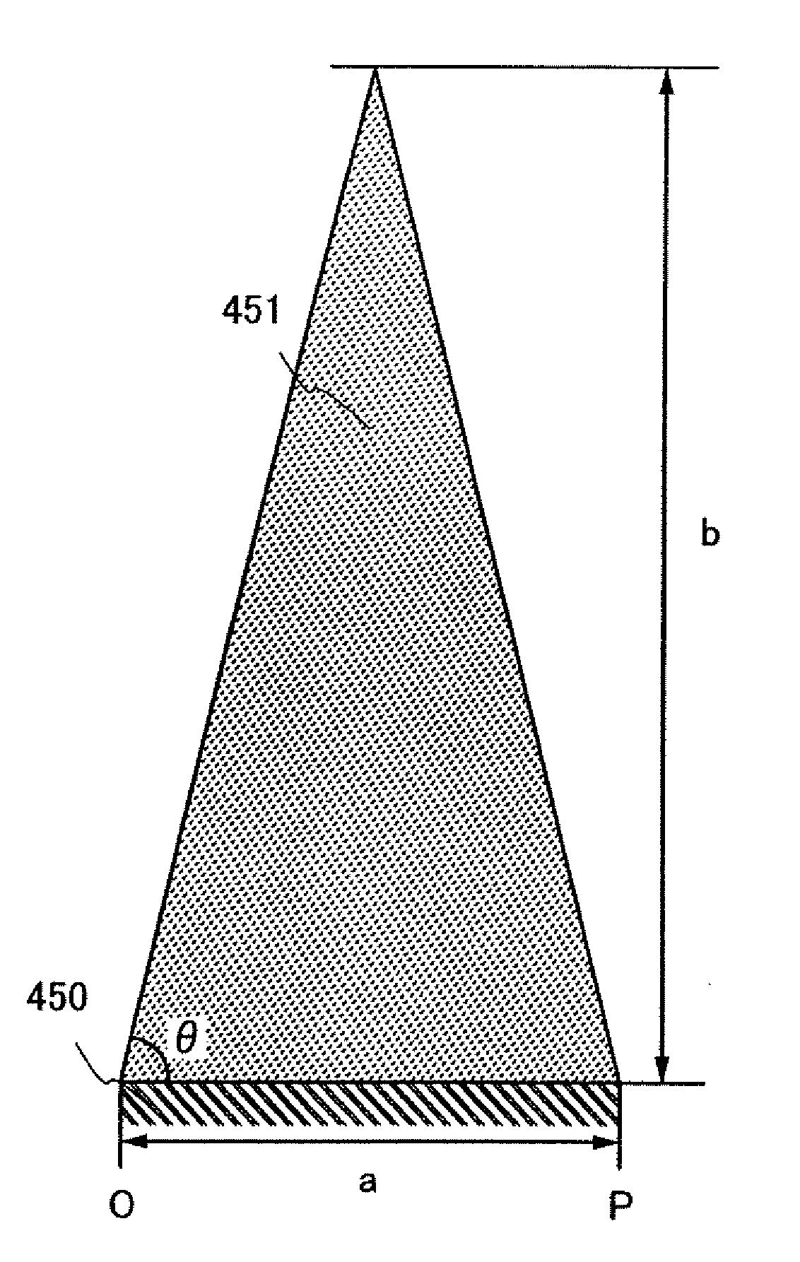
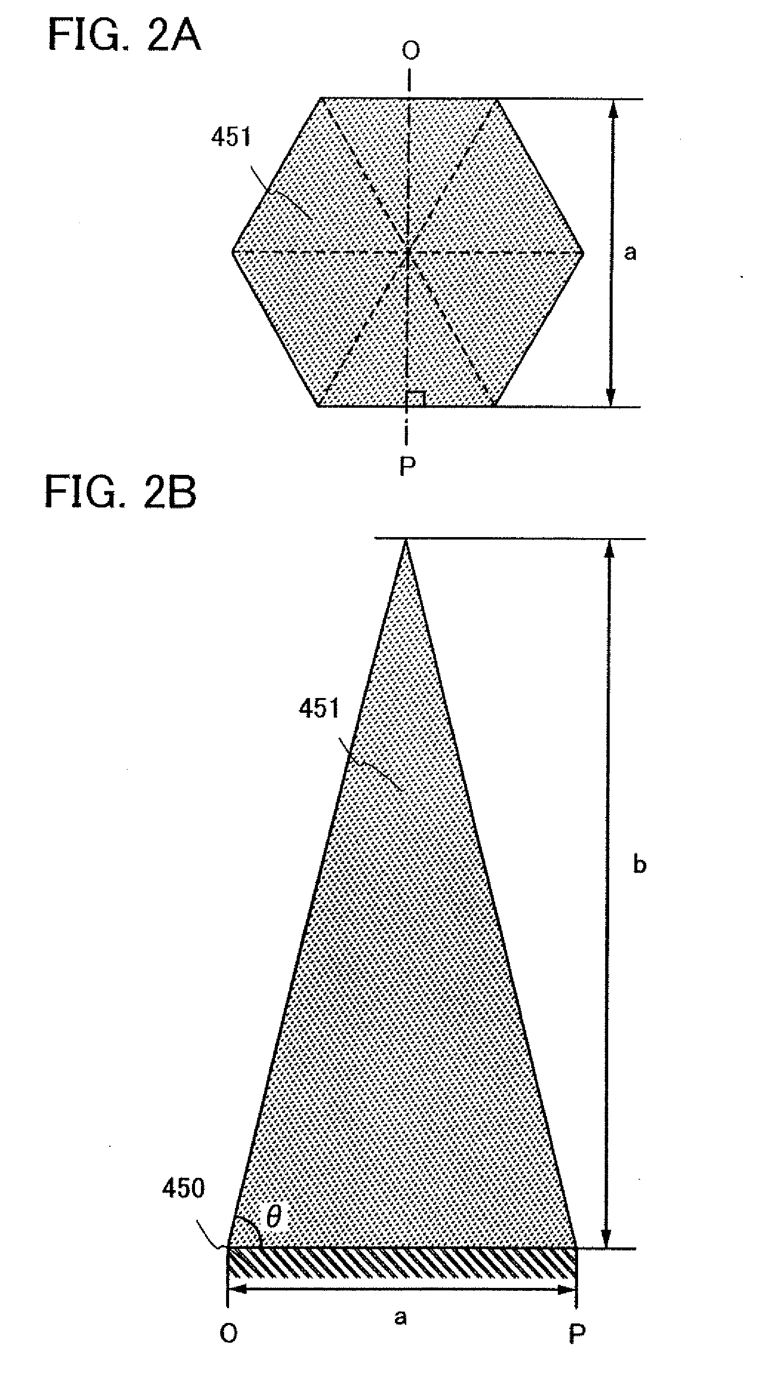
[0049]In Embodiment Mode 1, an anti-reflection layer provided for a PDP and an FED of the present invention will be described. Specifically, an example of an anti-reflection layer having an anti-reflection function capable of further reducing reflection of incident light from external on a surface of each of a PDP and an FED, and aimed at providing high visibility for the PDP and the FED will be described.

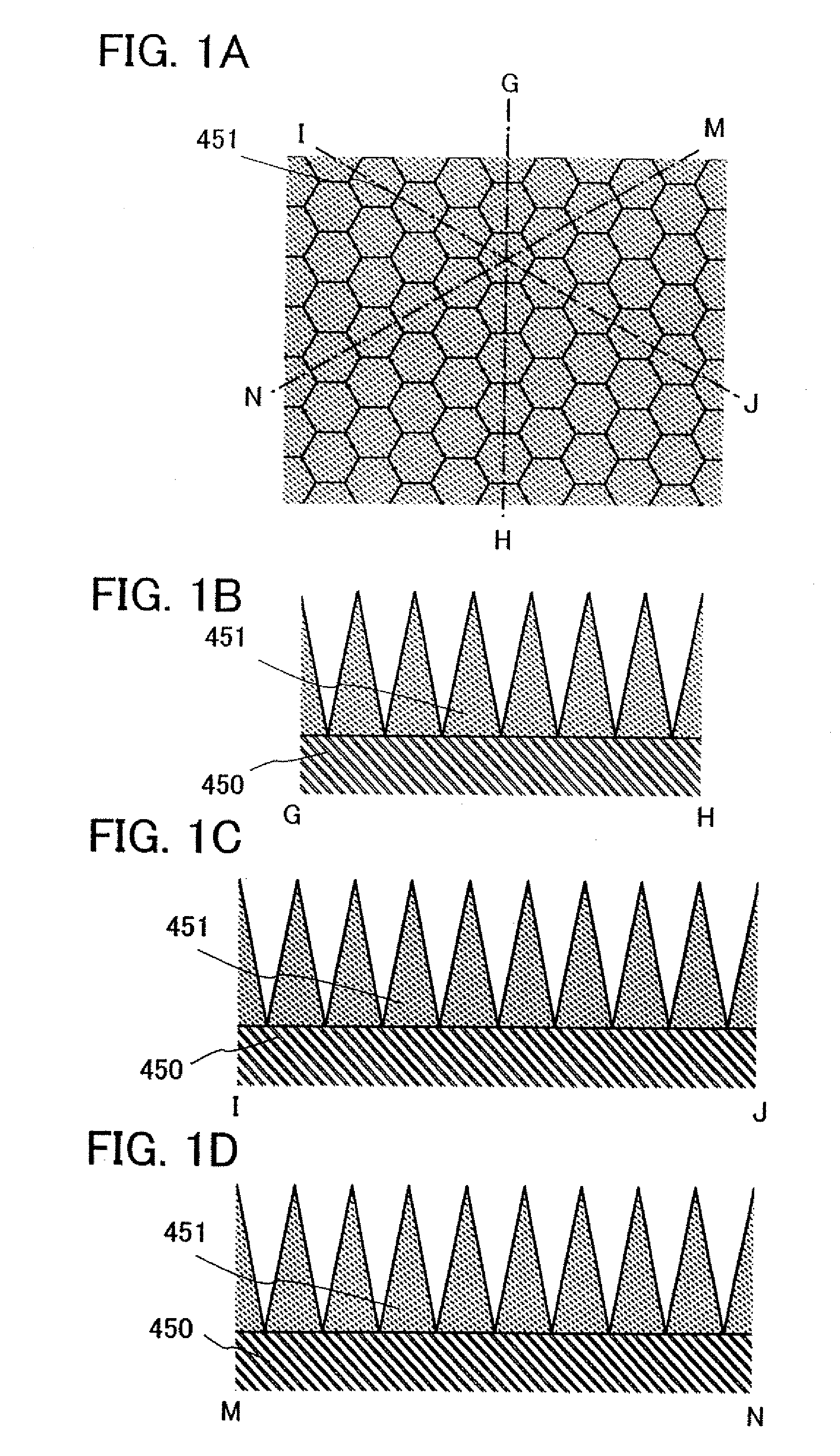
[0050]FIGS. 1A to 1D show a top view and cross-sectional views of an anti-reflection layer according to the present invention. In FIGS. 1A to 1D, a plurality of pyramid-shaped projections 451 are provided over a substrate 450 to serve as a display screen of a PDP or an FED. The anti-reflection layer according to the present invention includes the plurality of pyramid-shaped projections 451. FIG. 1A is a top view of a PDP or an FED of this embodiment mode. FIG. 1B is a cross-sectional view taken along line G-H in FIG. 1A, FIG. 1C is a cross-sectional view taken along line I-J in FIG...

embodiment mode 2

[0083]In Embodiment Mode 2, a PDP having an anti-reflection function capable of further reducing reflection of incident light from external and having excellent visibility will be described. That is, a structure of a PDP which includes a pair of substrates, at least a pair of electrodes provided between the pair of substrates, a phosphor layer provided between the pair of electrodes, and an anti-reflection layer provided on an outer side of one substrate of the pair of substrates will be described in detail.

[0084]In this embodiment mode, a surface discharge PDP of alternating current discharge type (AC type) is shown. FIG. 9A shows an enlarged diagram of a pyramid-shaped projection 101. As shown in FIG. 9B, in a PDIP, a front substrate 110 and a back substrate 120 face each other, and the periphery of the front substrate 110 and the back substrate 120 is sealed with a sealant (not shown). In addition, a region enclosed by the sealant, the front substrate 110, and the back substrate ...

embodiment mode 3

[0136]Embodiment Mode 3 will describe an FED having an anti-reflection function capable of reducing reflection of incident light from external and having excellent visibility. That is, a structure of an FED including a pair of substrates, a field emission element provided over one substrate of the pair of substrates, an electrode provided on the other substrate of the pair of substrates, a phosphor layer which is in contact with the electrode, and an anti-reflection layer provided on an outer side of the other substrate will be described in detail.

[0137]The FED is a display device in which phosphors are exited by an electron beam to emit light. The FED can be classified into a diode-type FED, a triode-type FED, and a tetrode-type FED according to the configurations of electrodes.

[0138]The diode-type FED has a structure where a rectangular cathode electrode is formed on a surface of a first substrate while a rectangular anode electrode is formed on a surface of a second substrate, an...


PUM

PropertyMeasurementUnit
Fractionaaaaaaaaaa
Heightaaaaaaaaaa
Heightaaaaaaaaaa

Abstract

To provide a PDP and an FED with high visibility, having an anti-reflection function capable of reducing reflection of incident light from external. An anti-reflection layer including a plurality of pyramid-shaped projections, apexes of which are provided at equal intervals and in which each side of a base which forms a pyramid shape of one of the plurality of pyramid-shaped projections is in contact with a side of a base which forms a pyramid shape of an adjacent pyramid-shaped projection, is included. In other words, one pyramid-shaped projection is surrounded by other pyramid-shaped projections, and the base of the pyramid-shaped projection shares a side of a base with the base of the adjacent pyramid-shaped projection.

Description

TECHNICAL FIELD[0001]The present invention relates to a plasma display panel and a field emission display each having an anti-reflection function.BACKGROUND ART[0002]In various displays (a plasma display panel (hereinafter referred to as a POP), a field emission display (hereinafter referred to as an FED), and the like), there may be a case where it becomes hard to see images of a display screen due to reflection of its surroundings by surface reflection of incident light from external or the like, so that visibility is decreased. This is a considerable problem particularly when the size of the display device is increased or the display device is used outdoors.[0003]In order to prevent such reflection of incident light from external, a method for providing an anti-reflection film for display screens of a PDP and an FED has been employed. For example, there is a method for providing an anti-reflection film that has a multilayer structure of stacked layers having different refractive ...

Claims


Application Information

Patent Timeline
IPC IPC(8): G02B27/00H01J17/49H01J1/62B82B3/00B82Y20/00B82Y40/00B82Y99/00G02B1/11G02B1/118G09F9/00G09F9/313H01J11/24H01J11/44H01J29/88H01J31/12
CPCH01J11/12H01J2211/442H01J29/896H01J11/44
Inventor NISHIDA, JIROEGI, YUJINISHI, TAKESHIYAMAZAKI, SHUNPEI
Owner SEMICON ENERGY LAB CO LTD
Why Eureka
Try Eureka