Method and circuit for low-power detection of solder-joint network failures in digital electronic packages

a technology of solder-joint network and low-power detection, which is applied in the direction of individual semiconductor device testing, emergency protective arrangements for limiting excess voltage/current, instruments, etc., can solve the problems of reduced reliability, prone to connection failure, and major reliability problems of solder-joint connections

Inactive Publication Date: 2008-06-19
RIDGETOP GROUP
View PDF17 Cites 50 Cited by
  • Summary
  • Abstract
  • Description
  • Claims
  • Application Information

AI Technical Summary

Benefits of technology

[0014]The present invention provides a low power circuit and method for reliable detection of in-situ failures or precursors to failures in operational solder-joint networks on actual operational devices and packages in the field. The circuit can monitor the entire solder-joint network for a digital electronic package including internal and external solder-joint connections. The detected failure or precursor of a selected monitor solder-joint network(s) is an indicator of the integrity of other operational solder-joint networks in the package, on the PWB or between PWBs.
[0015]This is accomplished by first holding one s...

Problems solved by technology

Solder-joint connections are a major reliability problem in electronic packaging.
In particular, the connections provided by connectors and cable harnesses, are prone to connection failure because of a fracture or high-resistance contact such as that between a connector and a cable-harness pin.
The increased number of pins on the packages is necessary to support the evolving complexity of circuits; however, one of the drawbacks of the increase is reduced reliability.
These “2-wire” and or “4-wire” techniques for direct measurement of solder-joint resistance have a number of limitations.
Therefore, the tests are limited to the extern...

Method used


Image

  • Method and circuit for low-power detection of solder-joint network failures in digital electronic packages
  • Method and circuit for low-power detection of solder-joint network failures in digital electronic packages
  • Method and circuit for low-power detection of solder-joint network failures in digital electronic packages

Examples


Embodiment Construction

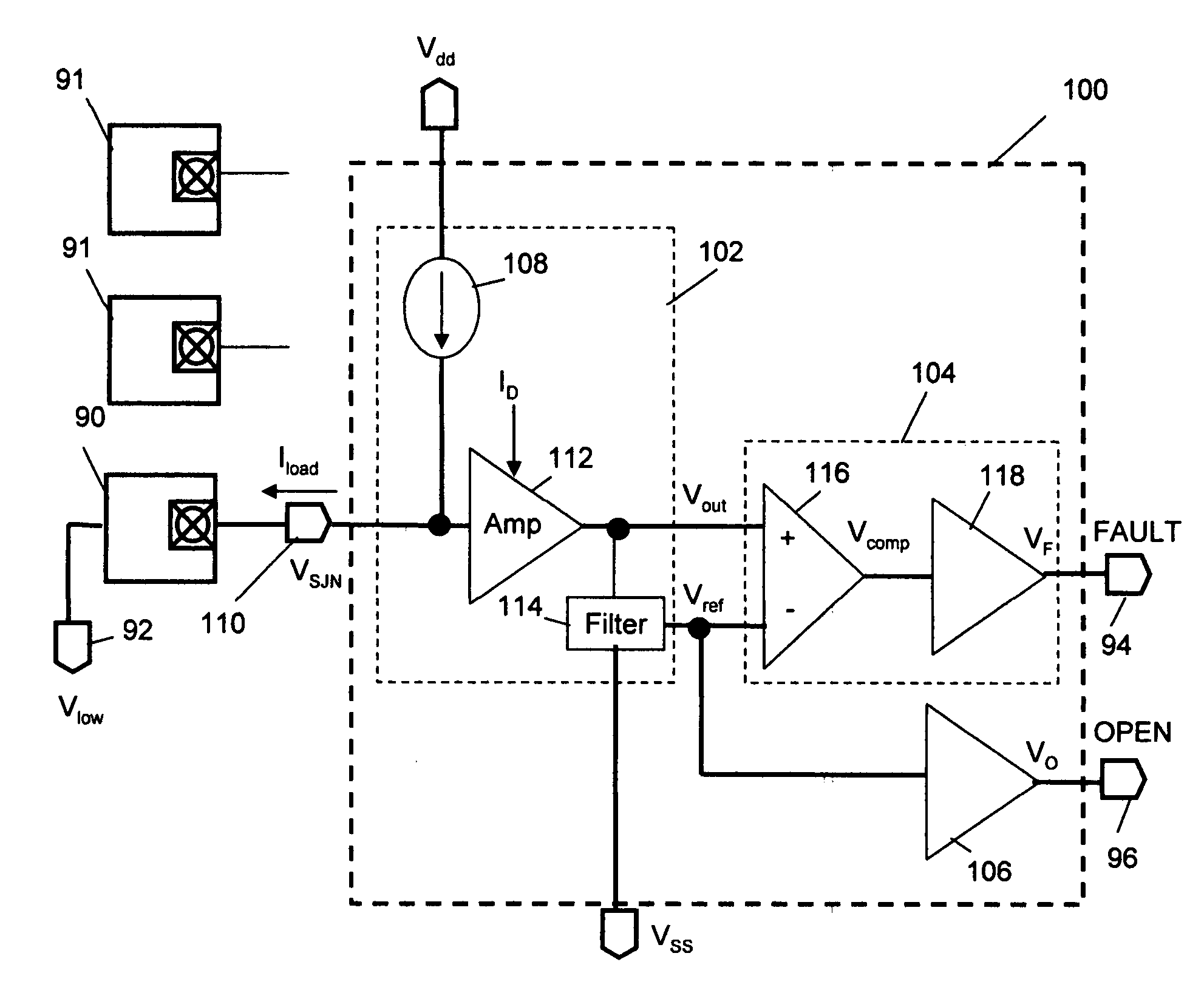
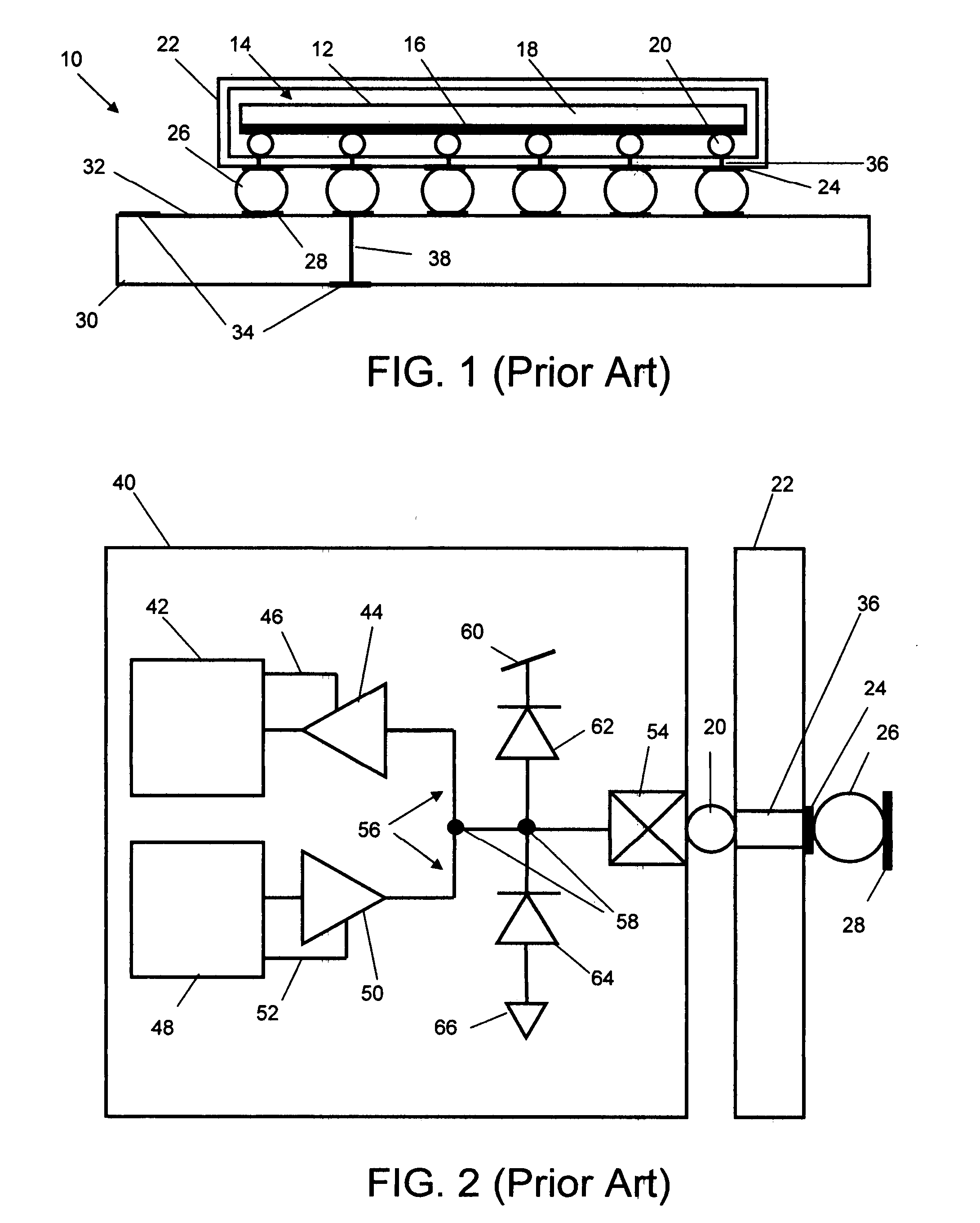
[0033]The present invention provides a low power circuit and method for detecting in-situ failures or precursors to failures in solder-joint networks on actual operational devices and packages in the field. The circuit can detect failures in a solder-joint network defined from the logic inside the die of an FPGA or microcontroller, through the internal and external solder-joint connections to circuit connections on a PWB in actual operational devices and packages in the field. The detected failure or precursor of a selected monitor solder-joint network(s) is an indicator of the integrity of other operational solder-joint networks in the package, on the PWB or between PWBs.

[0034]This is accomplished by first holding one side of a designated monitor solder-joint network at a low voltage including a steady-state component and noise, suitably by pulling the write logic output buffer on the die low. There is a large variation between the steady-state low-voltage (voltage-low) of transist...


PUM


Abstract

A low power circuit and method for detects in-situ failures or precursors to failures in solder-joint networks on actual operational devices and packages in the field. An amplifying detector such as provided by a common-gate transistor sources current to the network to generate a signal voltage and a reference voltage that is sensitive to the low voltage applied to the other side of the network. Generation of this self-adjusting reference voltage makes the detection circuit insensitive to the network low-voltage. Additional power savings and performance gains can be provided with the addition of a differential amplifier to set a fixed bias point and a level shifter to cancel noise. The detected failure or precursor of a selected monitor solder-joint network(s) is an indicator of the integrity of other operational solder-joint networks in the package, on the PWB or between PWBs.

Description

CROSS-REFERENCE TO RELATED APPLICATIONS[0001]This application claims benefit of priority under 35 U.S.C. 119(e) to U.S. Provisional Application Nos. 60 / 875,584 entitled “Method and circuit for the detection of solder-joint failures in digital electronic packages in a manner which is insensitive to the steady-state voltage level to the monitored solder-joint network and which suppresses both random and common-mode noise” filed on Dec. 19, 2006 and 60 / 879,518 entitled “Method and circuit for low-power detection of solder-joint failures in digital electronic packages in a manner which is insensitive to the steady-stage voltage level of the monitored solder joint networks and which suppresses noise” filed on Jan. 10, 2007, the entire contents of which are incorporated by reference.GOVERNMENTAL RIGHTS[0002]This invention was made with Government support under Contract N68335-06-C-0346 awarded by Naval Air Warfare Center AD (LKE). The Government has certain rights in this invention.BACKGR...

Claims


Application Information

Patent Timeline
IPC IPC(8): H02H9/04G01R31/26
CPCG01R31/048G01R31/71
Inventor MARIANI, GIORGIOHOFMEISTER, JAMES P.JUDKINS, JUSTIN B.
Owner RIDGETOP GROUP
Why Eureka
Try Eureka