Method for recess etching

a recess etching and recess technology, applied in the field of recess etching, can solve the problems of reducing the ratio of vertical to lateral etch distance, requiring greater vertical etch to lateral etch ratio, tighter constraints placed on the etch process used to form these structures, etc., to achieve the effect of improving the requirement of lateral to vertical etch ratio

Inactive Publication Date: 2008-06-19
APPLIED MATERIALS INC
View PDF15 Cites 18 Cited by
  • Summary
  • Abstract
  • Description
  • Claims
  • Application Information

AI Technical Summary

Benefits of technology

[0009]Methods for recess etching are provided herein that advantageously improve lateral to vertical etch ratio requirements, thereby enabling deeper recess etching while maintaining relatively shallow vertical etch depths. Such enhanced lateral etch methods advantageously provide benefits for numerous applications where lateral to vertical etch depth ratios are constrained or where recesses or cavities are desired to be formed. In some embodiments, a method of recess etching includes pr

Problems solved by technology

However, as the technology nodes continue to shrink, for example from 65 nm nodes to 45 nm and even 32 nm nodes, tighter constraints are placed upon the etch processes utilized to form these structures.
As such, the ratio of vertical to lateral etch distance decreases, thereby undesirably constraining conventional etch p

Method used


Image

  • Method for recess etching
  • Method for recess etching
  • Method for recess etching

Examples


Embodiment Construction

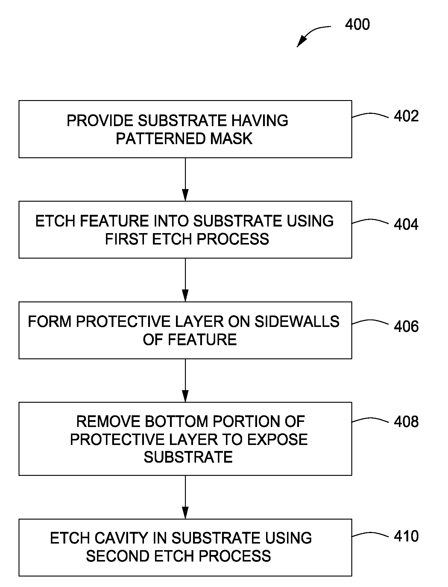
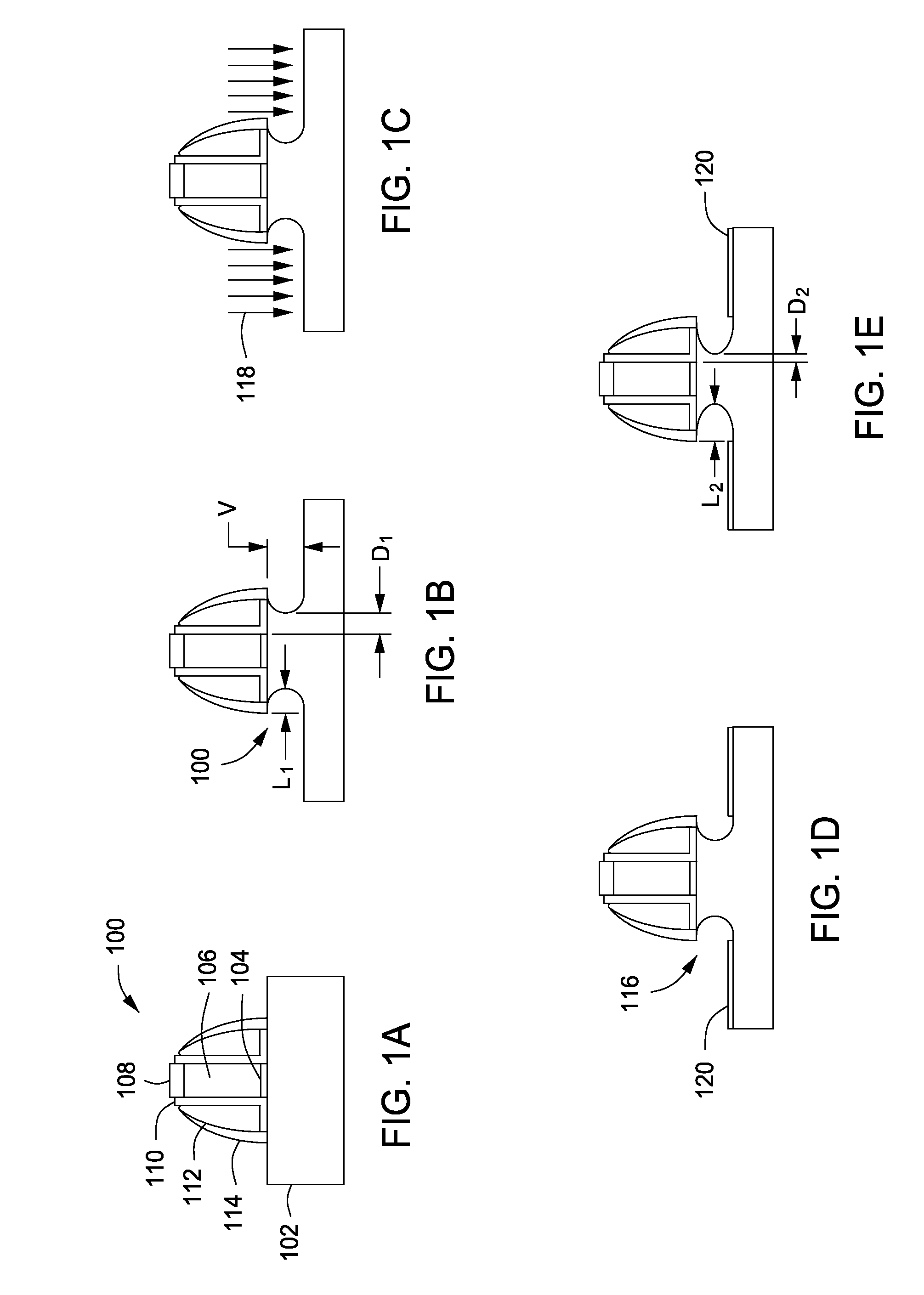
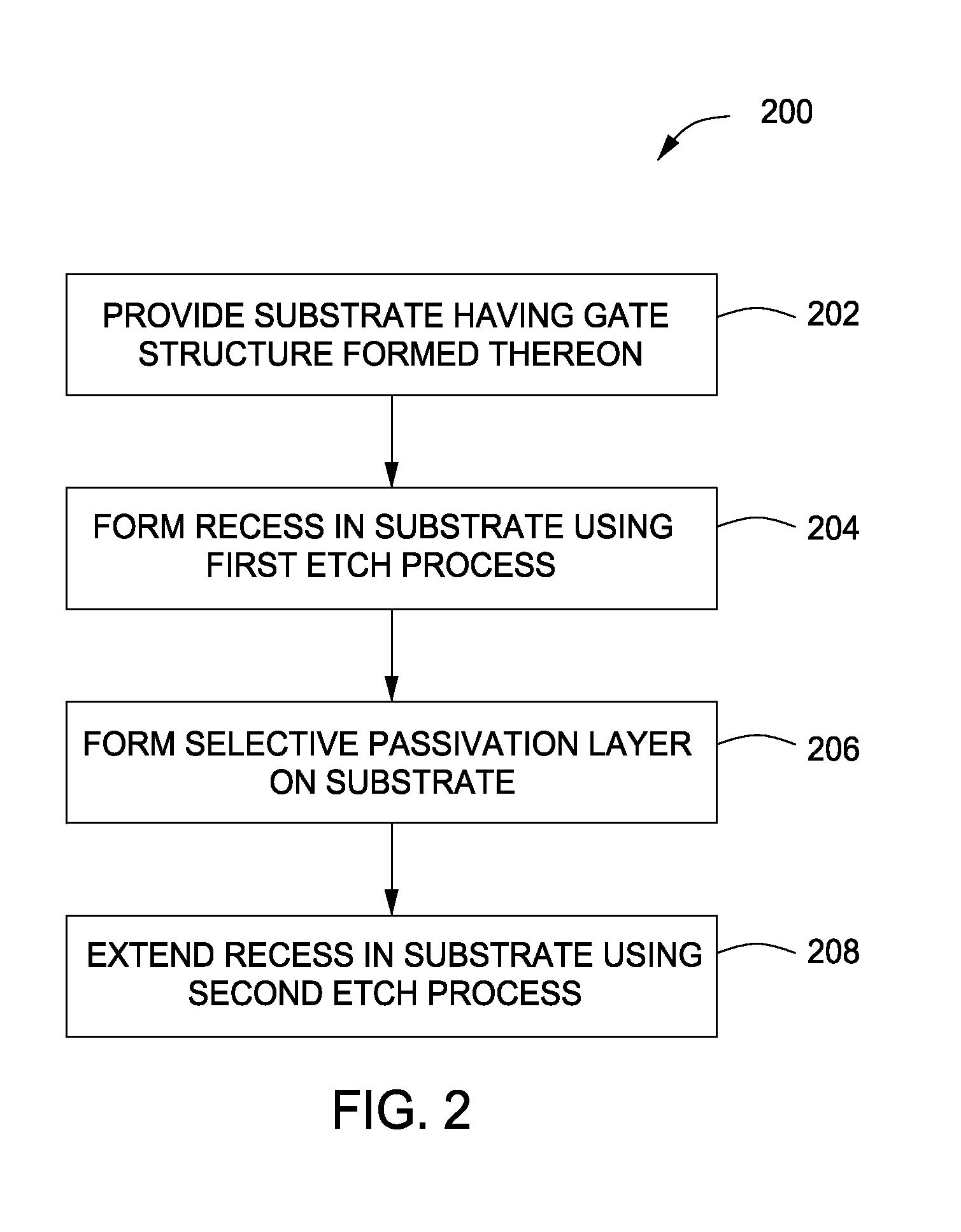
[0018]FIGS. 1A-E depict stages of fabrication of an illustrative gate structure in accordance with some embodiments of the present invention. FIG. 2 depicts one illustrative method for recess etching in accordance with some embodiments of the present invention and is described below with reference to FIGS. 1A-E. Suitable reactors that may be adapted for use with the teachings disclosed herein include, for example, the Decoupled Plasma Source (DPS®) ADVANTEDGE™ reactor, or the DPS® I or DPS® II etch reactor, all of which are available from Applied Materials, Inc. of Santa Clara, Calif. The DPS® ADVANTEDGE™, DPS® I or DPS® II reactors may also be used as processing modules of a CENTURA® integrated semiconductor wafer processing system, also available from Applied Materials, Inc. An illustrative embodiment of a suitable etch reactor is described below with respect to FIG. 5.

[0019]The method 200 begins at 202, where in one exemplary embodiment of the present invention, a substrate 102 h...


PUM


Abstract

Methods for recess etching are provided herein that advantageously improve lateral to vertical etch ratio requirements, thereby enabling deeper recess etching while maintaining relatively shallow vertical etch depths. Such enhanced lateral etch methods advantageously provide benefits for numerous applications where lateral to vertical etch depth ratios are constrained or where recesses or cavities are desired to be formed. In some embodiments, a method of recess etching includes providing a substrate having a structure formed thereon; forming a recess in the substrate at least partially beneath the structure using a first etch process; forming a selective passivation layer on the substrate; and extending the recess in the substrate using a second etch process. The selective passivation layer is generally formed on regions of the substrate adjacent to the structure but generally not within the recess. The first and second etch processes may be the same or different.

Description

CROSS-REFERENCE TO RELATED APPLICATIONS[0001]This application claims the benefit of U.S. Provisional Patent Application entitled “METHOD FOR RECESS ETCHING,” having Ser. No. 60 / 869,832, and filed Dec. 13, 2006, which is hereby incorporated by reference.BACKGROUND[0002]1. Field[0003]Embodiments of the present invention generally relate to fabrication of devices on semiconductor substrates, and, more specifically, to methods for recess etching during the fabrication of such devices.[0004]2. Description of the Related Art[0005]Ultra-large-scale integrated (ULSI) circuits may include more than one million electronic devices (e.g., transistors) that are formed on a semiconductor substrate, such as a silicon (Si) wafer, and cooperate to perform various functions within the device. Typically, the transistors used in the ULSI circuits are complementary metal-oxide-semiconductor (CMOS) field effect transistors. A CMOS transistor typically has a source region, a drain region, and a channel re...

Claims


Application Information

Patent Timeline
IPC IPC(8): H01L21/311
CPCH01L21/3065H01L29/7848H01L29/66636H01L21/30655H01L21/308
Inventor SHEN, MEIHUACHEN, RONGWILLIAMS, SCOTT M.
Owner APPLIED MATERIALS INC
Why Eureka
Try Eureka