Use of a porous dielectric material as an etch stop layer for non-porous dielectric films

a dielectric film and porous material technology, applied in the direction of semiconductor devices, semiconductor/solid-state device details, electrical apparatus, etc., can solve the problems of increasing the difficulty of efficient routing of these signals across the device, and increasing the difficulty of etching, so as to improve device functionality and performance, the effect of reducing the variation of line height and minimal line resistan

Inactive Publication Date: 2008-06-19
ALSEPHINA INNOVATIONS INC
View PDF21 Cites 6 Cited by
  • Summary
  • Abstract
  • Description
  • Claims
  • Application Information

AI Technical Summary

Benefits of technology

[0012]In accordance with the present invention, the BEOL interconnect structures of the present invention have minimized line height variation and minimal line resistance variation. More particularly, the inventive BEOL interconnect structures have improved device functionality and performance due to the reduced effective dielectric constant, keff, of the overall BEOL stack compared with conventionally employed BEOL stacks.

Problems solved by technology

Efficient routing of these signals across the device can become more difficult as the complexity Efficient routing of these signals across the device can become more difficult as the complexity and number of integrated circuits are increased.
In typical trench or via-first integration strategies, one of the challenges during the creation of the line level structure in dual damascene processing is to minimize line height variations (and hence line resistance variance) within a wafer and within a lot.
These line height variations can arise owing to occasional etch rate non-uniformities within the employed plasma process dependent on pattern density and / or feature aspect ratio variations or due to variations in the interlevel dielectric (ILD) film thickness.
In addition to the above problem concerning prior art ESLs, there is an ongoing trend of replacing traditional ILDs with low-k dielectrics that are porous.
Since typically BEOL processing conditions would etch a low-k dielectric hardmask faster than the underlying porous low-k material, the issue in line height control and resistance variation is perhaps made even more severe for these technologies.

Method used


Image

  • Use of a porous dielectric material as an etch stop layer for non-porous dielectric films
  • Use of a porous dielectric material as an etch stop layer for non-porous dielectric films
  • Use of a porous dielectric material as an etch stop layer for non-porous dielectric films

Examples


first embodiment

7-oxabicyclo[2.2.1]heptane or 1,4-epoxycyclohexane (bp=119° C. at 713 mm Hg). One highly preferred fused ring species that is employed in the present invention is cyclopentene oxide (CPO).

[0035]The second precursor can also include a siloxane selected from tetramethylorthosilicate (TMOS), tetraethylorthosilicate (TEOS), vinyltriethoxysilane, allyltrimethoxysilane, vinyltrimethoxysilane, allyltriethoxysilane, phenyltriethoxysilane, and phenyltrimethoxysilane.

[0036]The porous OSG material is formed by providing a pore forming material such as a porogen during deposition. Although any deposition technique can be used in forming the OSG materials, the techniques disclosed in co-assigned U.S. Pat. Nos. 6,147,009, 6,497,963, 6,312,793, 6,441,491 and 6,479,110, the entirety of each reference is incorporated herein by reference, are particularly preferred herein.

[0037]The various OSG dielectrics may be deposited within the same reactor chamber without the need of breaking vacuum, or the var...

second embodiment

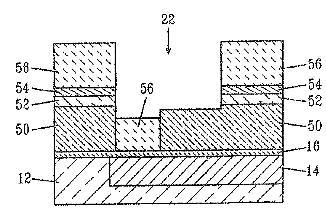
[0053]Next, oxide hard mask 54 is formed atop the non-porous hardmask 52 and an opening that is filled with a planarizing dielectric 56 is then formed by lithography, etching and deposition. The etching step includes any conventional etching process. Note that the etching process mentioned above which includes the fluorocarbon-based plasma etch can also be employed at this point of the present invention. The planarizing dielectric includes any material that can serve as a planarizing layer including for example, a non-photosensitive organic cross-linked polymer.

[0054]After forming the planarizing dielectric 56, an oxide cap 58 such as a low temperature oxide and an optional antireflective coating 60 are formed by known deposition methods. A patterned photoresist 62 containing a line pattern is formed by deposition and lithography. Several prior art etch processes are then used to etch layers 60, 58, and 56 which is subsequently followed by the inventive etch to process layers 54 and...


PUM

PropertyMeasurementUnit
pressureaaaaaaaaaa
dielectric constantaaaaaaaaaa

Abstract

Interconnect structures possessing a non-porous (dense) low-k organosilicate glass (OSG) film utilizing a porous low-k OSG film as an etch stop layer or a porous low-k OSG film using a non-porous OSG film as a hardmask for use in semiconductor devices are provided herein. The novel interconnect structures are capable of delivering improved device performance, functionality and reliability owing to the reduced effective dielectric constant of the stack compared with that of those conventionally employed and also because of the relatively uniform line heights made feasible by these unique and seemingly counterintuitive features. The present invention also provides a fluorocarbon-based dual damascene etch process that achieves selective etching of a dense low-k OSG films relative to that of a porous low-k OSG film owing to the tunability of the gas-phase fluorine:carbon ratio (gas dissociation) and ion current below a critical threshold and given the larger carbon content of the porous film relative to that of the dense film.

Description

RELATED APPLICATIONS[0001]This application is a divisional of U.S. patent application Ser. No. 10 / 845,718, filed May 14, 2004.DESCRIPTION[0002]1. Field of the Invention[0003]The present invention generally relates to semiconductor integrated circuits (ICs), and more particularly to semiconductor interconnect structures, including multilevel interconnect structures, in which advanced dual damascene processing enables using a porous low-k dielectric material as an etch stop layer (ESL) for a non-porous (dense) low-k dielectric film, or using a non-porous (dense) low-k dielectric film as a hardmask for a porous low-k dielectric material. The term “low-k” is used throughout the present application to denote an insulator having a dielectric constant of less than silicon dioxide, i.e., less than about 4.0. All dielectric constant values are measured in a vacuum unless otherwise specified herein.[0004]2. Background of the Invention[0005]Currently, semiconductor devices include a plurality ...

Claims


Application Information

Patent Timeline
Patent Type & Authority Applications(United States)
IPC IPC(8): H01L21/302H01L21/768H01L23/48H01L23/532
CPCH01L21/76807H01L21/76808H01L21/76829H01L23/53295H01L21/76835H01L23/5329H01L21/76834H01L2924/0002H01L2924/00
Inventor FULLER, NICHOLAS C.M.DALTON, TIMOTHY J.
Owner ALSEPHINA INNOVATIONS INC
Why Eureka
Try Eureka