Use of a porous dielectric material as an etch stop layer for non-porous dielectric films
a dielectric film and porous material technology, applied in the direction of semiconductor devices, semiconductor/solid-state device details, electrical apparatus, etc., can solve the problems of increasing the number of integrated circuits, affecting the functionality of the device, and the efficient routing of these signals across the device can become more difficult, so as to achieve the effect of minimal line resistance variation, minimal line height variation, and improved device functionality and performan
- Summary
- Abstract
- Description
- Claims
- Application Information
AI Technical Summary
Benefits of technology
Problems solved by technology
Method used
Image
Examples
first embodiment
[0035] Especially useful, are species containing fused rings, at least one of which contains a heteroatom, preferentially oxygen. Of these species, the most suitable are those that include a ring of a size that imparts significant ring strain, namely rings of 3 or 4 atoms and / or 7 or more atoms. Particularly attractive, are members of a class of compounds known as oxabicyclics. Among the readily available examples of these, are 6-oxabicyclo[3.1.0]hexane or cyclopentene oxide (bp=102° C. at 760 mm Hg); 7-oxabicyclo[4.1.0]heptane or cyclohexene oxide (bp=129° C. at 760 mm Hg); 9-oxabicyclo[6.1.0]nonane or cyclooctene oxide (bp=55° C. at 5 mm Hg); and 7-oxabicyclo[2.2.1]heptane or 1,4-epoxycyclohexane (bp=119° C. at 713 mm Hg). One highly preferred fused ring species that is employed in the present invention is cyclopentene oxide (CPO).
[0036] The second precursor can also include a siloxane selected from tetramethylorthosilicate (TMOS), tetraethylorthosilicate (TEOS), vinyltriethoxysil...
second embodiment
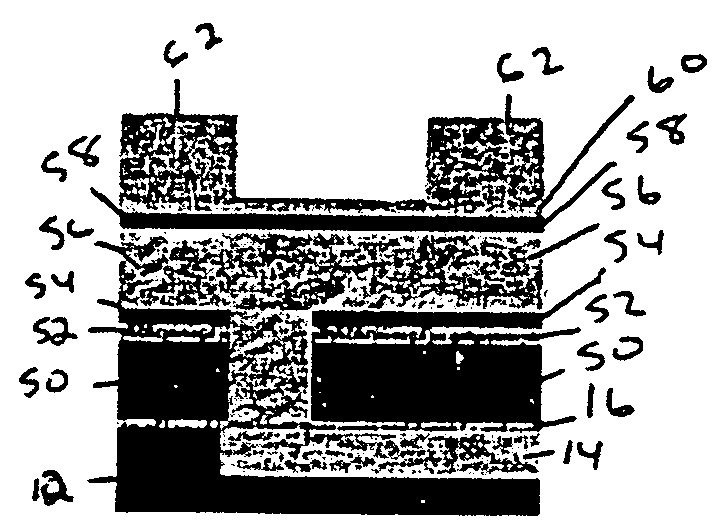
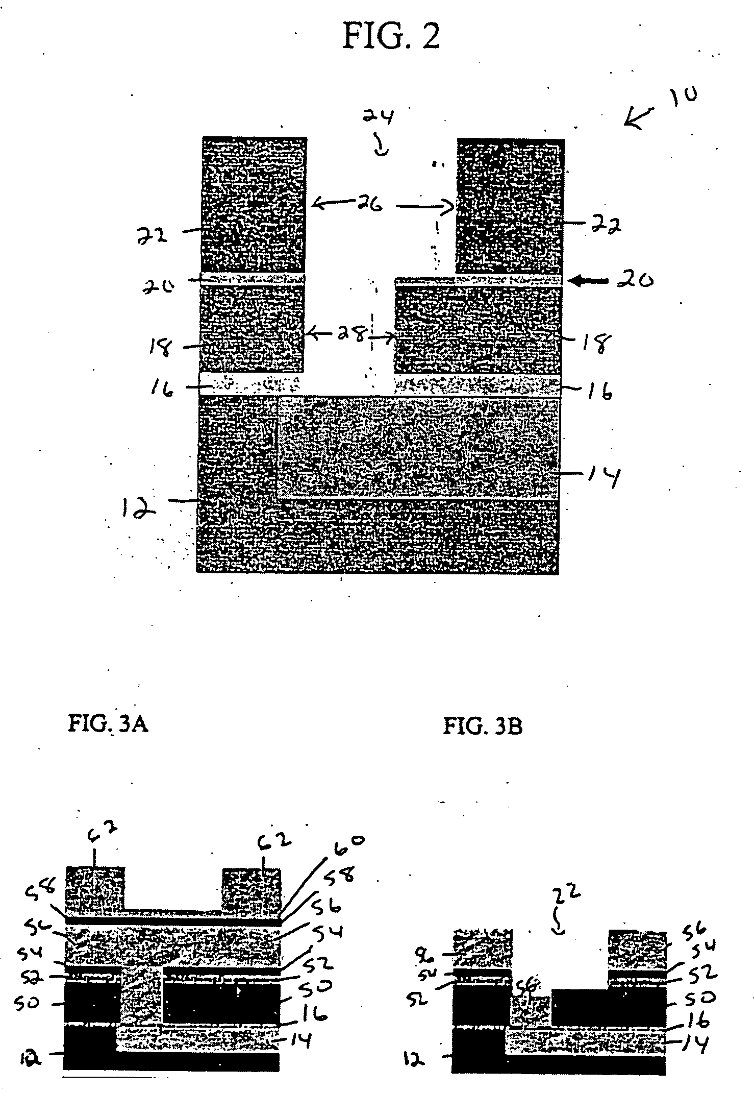
[0054] Next, oxide hard mask 54 is formed atop the non-porous hardmask 52 and an opening that is filled with a planarizing dielectric 56 is then formed by lithography, etching and deposition. The etching step includes any conventional etching process. Note that the etching process mentioned above which includes the fluorocarbon-based plasma etch can also be employed at this point of the present invention. The planarizing dielectric includes any material that can serve as a planarizing layer including for example, a non-photosensitive organic cross-linked polymer.
[0055] After forming the planarizing dielectric 56, an oxide cap 58 such as a low temperature oxide and an optional antireflective coating 60 are formed by known deposition methods. A patterned photoresist 62 containing a line pattern is formed by deposition and lithography. Several prior art etch processes are then used to etch layers 60, 58, and 56 which is subsequently followed by the inventive etch to process layers 54 a...
PUM
 Abstract
Description
Claims
Application Information


