Semiconductor device manufacturing apparatus and method

Active Publication Date: 2008-06-19
MICRON TECH INC
View PDF5 Cites 10 Cited by
  • Summary
  • Abstract
  • Description
  • Claims
  • Application Information

AI Technical Summary

Benefits of technology

[0017]It is an object of the present invention to solve the aforementioned problems. One object of the invention is to provide a retainer ring structure which is capable of stabilizing the uniformity of the amount of polishing in the surface of a wafer even if a retainer ring is worn.
[0020]The invention disclosed in Patent Document 1 forms a groove in a retainer ring to limit the influence of heat generation in polishing, which has been confirmed to be caused by heat generation that is associated with an increase in the width of the retainer ring. Patent Document 1 describes that such a groove improves limiting the influence of heat generation caused by friction and improves the efficiency of the supply and exhaustion of polishing material.
[0022]The invention disclosed in Patent Document 2 improves the efficiency of supplying polishing material by forming a groove in a retainer ring and supplying polishing material from the inside of the groove. Patent Document 2 describes in Paragraph [0048] that an inclination is formed in the groove for supplying the polishing material to ensure a pressing area on the inner periphery of the retainer ring.
[0024]As described above, while two known documents related to the present invention are presented by way of example, they are unable to produce the results which the object of the present invention is designed to achieve. Taking into consideration the limitations of both inventions described in the two patent documents, the present invention provides a unique configuration for efficiently producing definite effects.

Problems solved by technology

As a result, the effective pressure of retainer ring 1 (contact pressure with polishing pad 8) increases, causing a change in the polishing rate near the edge of semiconductor wafer 5, and causing non uniform polishing of the wafer surface to be exacerbated.
However, while the exacerbation of uniformity can be restrained to some degree, this action requires continuous condition adjustments and significantly hampers productivity.
Also, while more frequent replacements of retainer ring 1 is also taken into consideration, this is not a realistic solution.
Since aging changes in within-wafer uniformity become obvious at the initial stage after the start of use, it can be said that the action involving a replacement of retainer ring 1 at an earlier stage cannot solve the aforementioned problem.
However, this action simply causes an initial wear stage, in which the within-wafer uniformity changes in large as shown in FIG. 3 and which continues for a longer period, and does not constitute an effective solution.

Method used


Image

  • Semiconductor device manufacturing apparatus and method
  • Semiconductor device manufacturing apparatus and method
  • Semiconductor device manufacturing apparatus and method

Examples


first exemplary embodiment

[0039]FIG. 4 is a plan view seen from a surface of a retainer ring which comes into contact with a polishing pad, used in a first exemplary embodiment of the present invention. Grooves 2a, 2b are formed in a surface of retainer ring 1 which comes into contact with polishing pad 8.

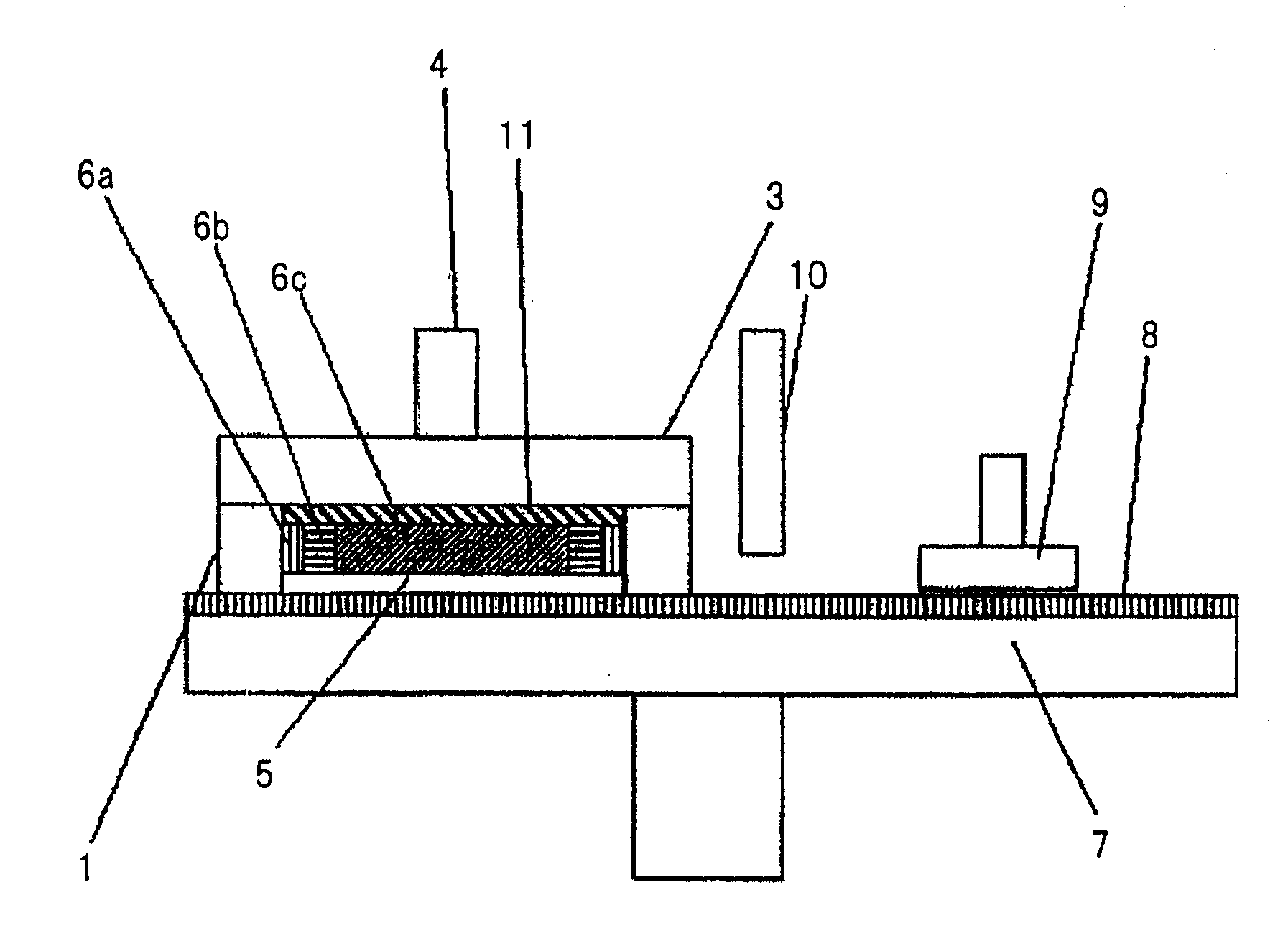
[0040]As previously shown in FIG. 1, such retainer ring 1 is mounted to head 3 which is the main component of a CMP apparatus. Spindle 4 is provided above head 3 for applying a rotating motion to head 3. Membrane 6 is also mounted to head 3, in addition to retainer ring 1, for chucking semiconductor wafer 5 and for applying a pressure on the back surface of semiconductor wafer 5 during polishing. Membrane 6 is divided into several regions, such that different pressures can be applied by membrane 6a to the outermost region of the wafer, to membrane 6b for a region inside of membrane 6a, and to membrane 6c for a wide region of the wafer except for the outer peripheral side. In this way, the surface of semicon...

second exemplary embodiment

[0059]Next, a description will be given of a second exemplary embodiment of the present invention, where the description will be given of only parts different from the CMP apparatus of the first exemplary embodiment.

[0060]FIG. 7 is a cross-sectional view showing the main portion of a retainer ring used in the second exemplary embodiment of the present invention.

[0061]In this exemplary embodiment, the bottom surface of each groove 2b concentrically formed in a surface of retainer ring 1 in contact with polishing pad 8 is machined into a concavely curved shape.

[0062]For example, when the depth of each groove 2b is chosen to be 0.1 mm, 0.2 mm, or 0.3 mm in order inwardly from the outer periphery of retainer ring 1, the bottom surface of each groove 2b is formed with curved area 17 having radius R of approximately 0.05 mm.

[0063]When each groove 2b has a flat bottom surface, the groove is suddenly eliminated due to the advance of wear, and the shock is a concern at that time, but curved ...

third exemplary embodiment

[0065]Next, a description will be given of a third exemplary embodiment of the present invention. Likewise, the description will be given herein only of parts different from the CMP apparatus of the first exemplary embodiment.

[0066]FIG. 8 is a cross-sectional view showing a main portion of a retainer ring used in the third exemplary embodiment of the present invention.

[0067]In this exemplary embodiment, each of the grooves concentrically provided in the surface of retainer ring 1 in contact with polishing pad 8 has the same depth and is tapered toward the bottom of the groove. Specifically, each of the concentric grooves is a tapered groove 2c as shown in FIG. 8, and differs from the first exemplary embodiment in that there are grooves 2b which differ from each other in regard to depth.

[0068]The bottom surface of grooves 2c may be machined into a concavely curved surface as in the second exemplary embodiment.

[0069]Taking such a form of grooves, the correlation of a groove occupation...


PUM

PropertyMeasurementUnit
Pressureaaaaaaaaaa
Widthaaaaaaaaaa
Areaaaaaaaaaaa

Abstract

A semiconductor device manufacturing apparatus according to the present invention comprises a head for holding a semiconductor wafer, a retainer ring for surrounding the outer periphery of the semiconductor wafer held by the head, and a polishing pad for polishing a polished surface of the semiconductor wafer. This apparatus presses the polished surface of the semiconductor wafer against the polishing pad together with the retainer ring to polish the semiconductor wafer. The retainer ring used in the present invention has a surface that is in contact with the polishing pad, which increases a contact area of the retainer ring against the polishing pad in accordance with wear of the retainer ring.

Description

[0001]This application is based upon and claims the benefit of priority from Japanese patent application No. 2006-339904, filed on Dec. 18, 2006, the disclosure of which is incorporated herein in its entirety by reference.BACKGROUND OF THE INVENTION[0002]1. Field of the Invention[0003]The present invention relates to a semiconductor device manufacturing apparatus and method. More particularly, the present invention relates to a retainer ring provided in a CMP (Chemical Mechanical Polishing) apparatus for polishing a semiconductor wafer, and a method of manufacturing a semiconductor device using the CMP apparatus.[0004]2. Description of the Related Art[0005]An increasingly strict level of flatness has been required for the surface of semiconductor devices for patterning thereon in semiconductor device manufacturing steps as wires become finer and finer. Then, after the design rule of semiconductor devices was reduced to less than 0.35 μm, CMP apparatuses are generally used to directl...

Claims


Application Information

Patent Timeline
IPC IPC(8): B24B7/00B24B37/04B24B37/30H01L21/304
CPCB24B37/32
Inventor TORII, KOJI
Owner MICRON TECH INC
Why Eureka
Try Eureka