Semiconductor memory device
- Summary
- Abstract
- Description
- Claims
- Application Information
AI Technical Summary
Benefits of technology
Problems solved by technology
Method used
Image

Examples
Embodiment Construction
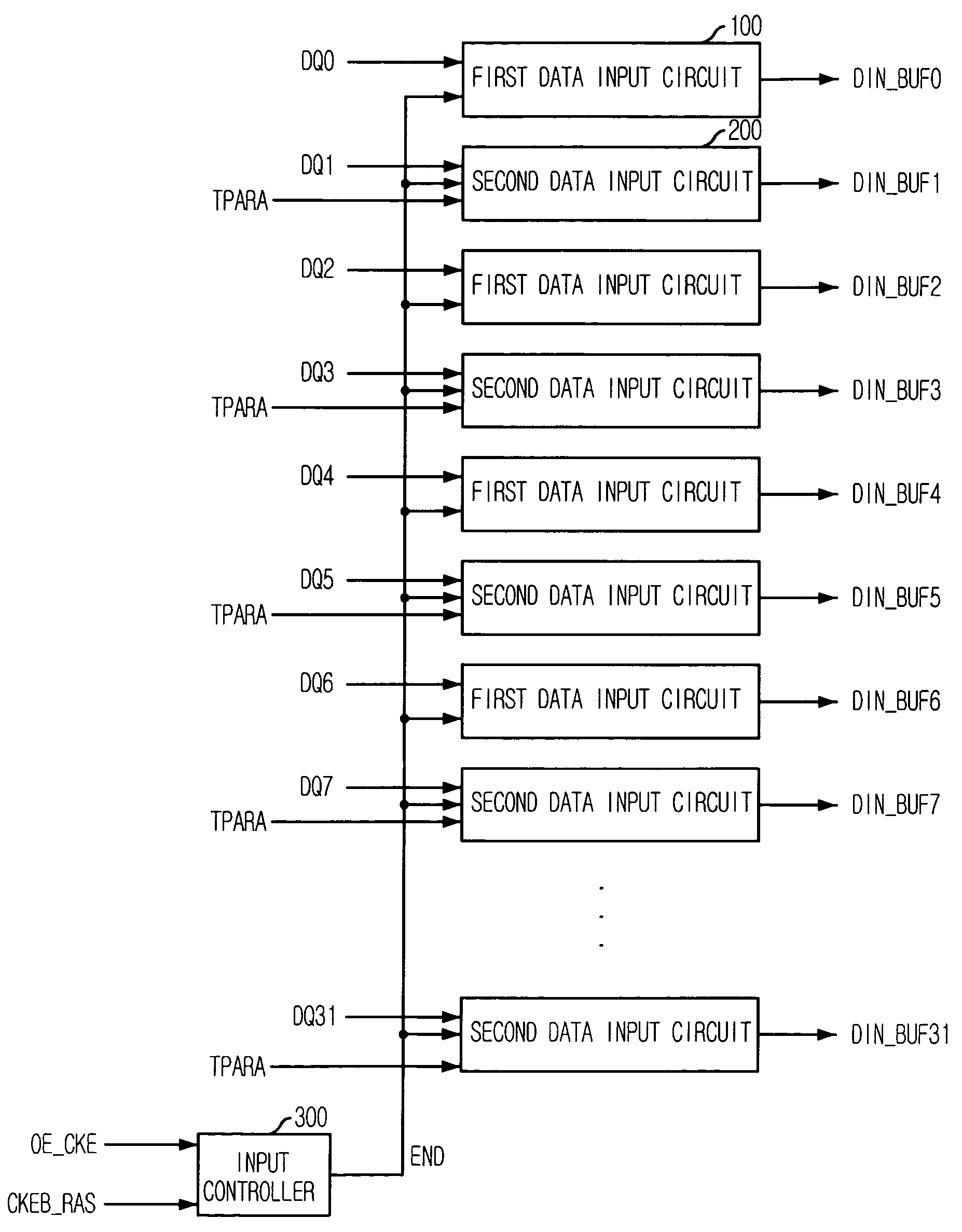
[0035]FIG. 6 is a block diagram of a semiconductor memory device in accordance with a preferred embodiment of the present invention.
[0036]Referring to FIG. 6, the semiconductor memory device of the present invention includes a first data input circuit 100 for receiving a data signal DQ0 and outputting it as an internal data signal DIN_BUF0, a second data input circuit 200 for receiving a data signal DQ1 and providing it as an internal data signal DIN_BUF1, and which is disabled in response to a test mode signal TPARA, and an input controller 300 for receiving control signals OE_CKE and CKEB_RAS and outputting an input control signal END to control input timing of the data signals DQ0 and DQ1 input to the first and the second data input circuits 100 and 200. The plurality of first data input circuits illustrated in FIG. 6 have the same configurations and the plurality of second input circuits also have the same configurations. Although it is assumed that a 32-bit data signal is input...
PUM
 Abstract
Description
Claims
Application Information
 - R&D Engineer
- R&D Manager
- IP Professional
- Industry Leading Data Capabilities
- Powerful AI technology
- Patent DNA Extraction
Browse by: Latest US Patents, China's latest patents, Technical Efficacy Thesaurus, Application Domain, Technology Topic.
© 2024 PatSnap. All rights reserved.Legal|Privacy policy|Modern Slavery Act Transparency Statement|Sitemap