Nanoelectronic structure and method of producing such

a technology of nanoelectronic structure and nanoelectronic junction, which is applied in the field of nanoelectronic junction and method of producing such, can solve the problems of access resistance and conductivity characteristics of prior art semiconductors in small dimensions, and achieve the effect of improving conductivity characteristics and improving/tailored pn junctions

Inactive Publication Date: 2008-06-26
QUNANO
View PDF68 Cites 140 Cited by
  • Summary
  • Abstract
  • Description
  • Claims
  • Application Information

AI Technical Summary

Benefits of technology

[0016]Thus, it is possible to provide new and improved nano-engineered structures for semiconductor devices, comprising nanoelements connected in series with volume elements with essentially larger dimensions having improved conductivity characteristics.
[0017]It is a further advantage of the embodiments of the invention to provide new and improved nano-engineered structures for semiconductor devices, comprising nanoelements connected in series with volume elements, wherein the structures comprise improved / tailored pn-junctions.

Problems solved by technology

Prior art semiconductors in small dimensions have drawbacks with regards to access resistance and conductivity characteristics.

Method used


Image

  • Nanoelectronic structure and method of producing such
  • Nanoelectronic structure and method of producing such
  • Nanoelectronic structure and method of producing such

Examples


Embodiment Construction

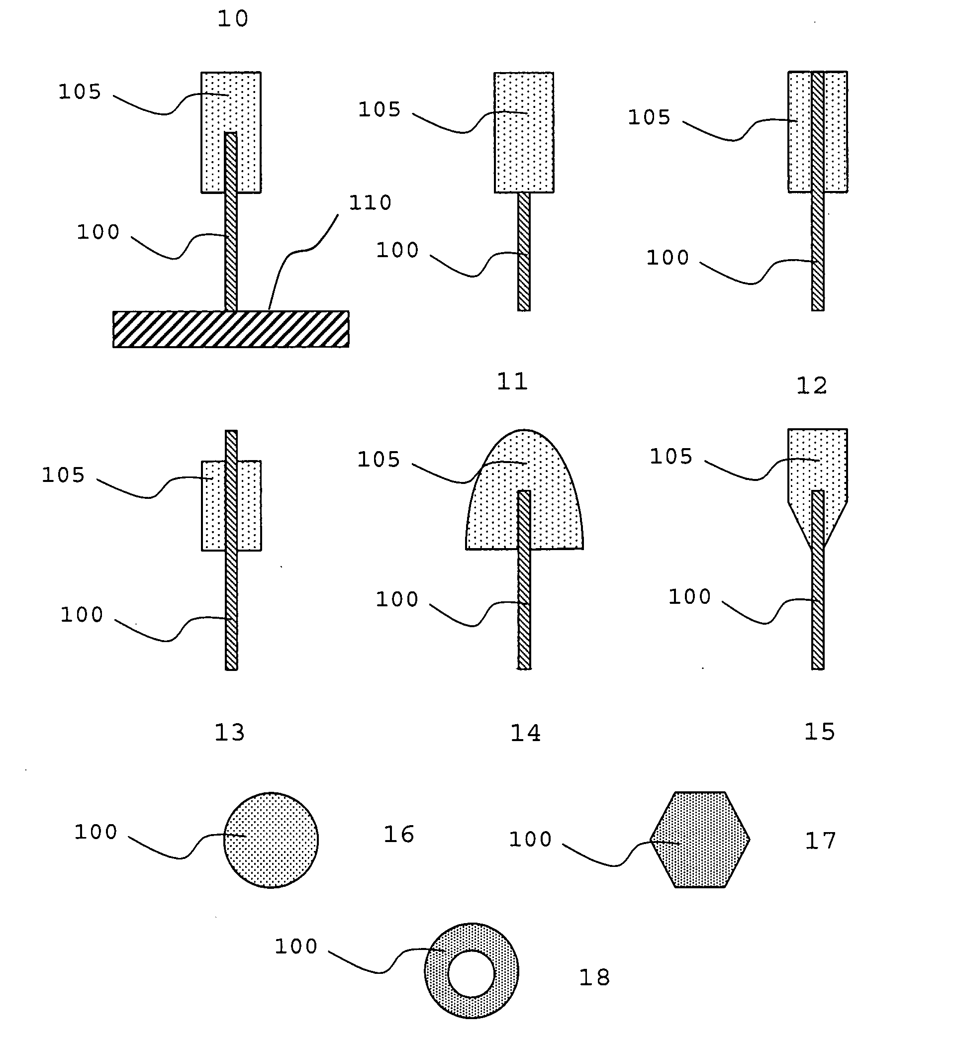
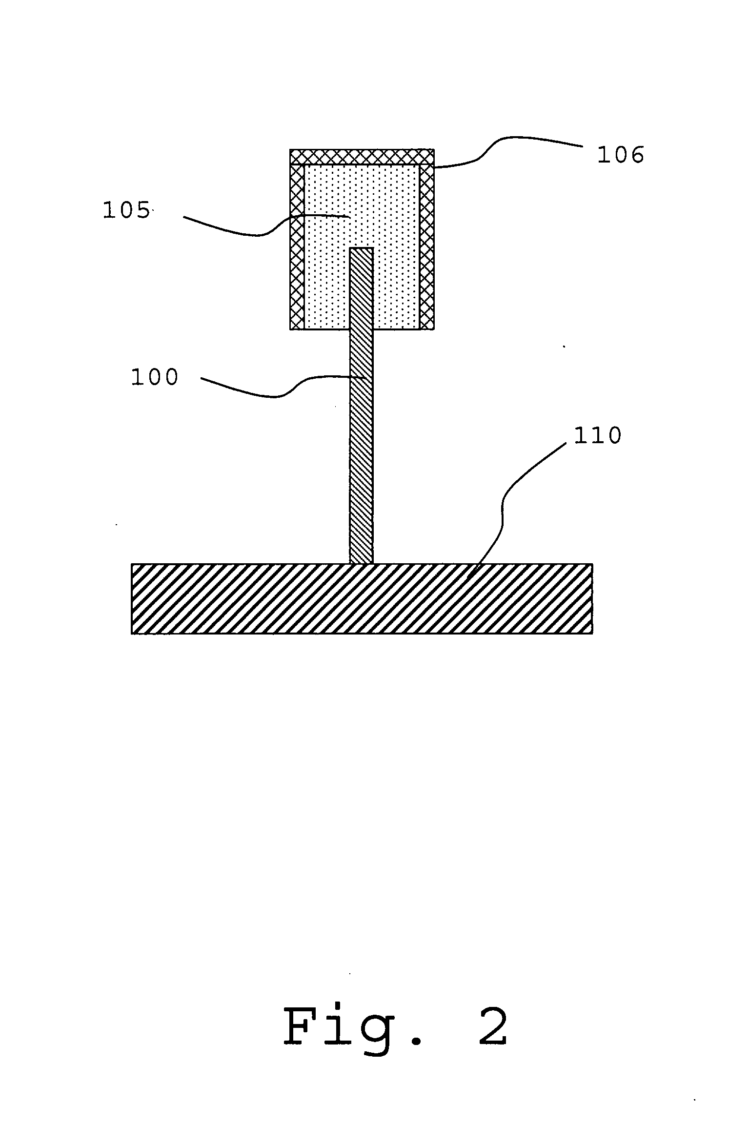
[0039]A semiconductor device according to the embodiments of the present invention opens new possibilities for the implementation of different electronic and photonic semiconductor devices, particularly in small dimensions.

[0040]The embodiments of present invention decrease general difficulties associated with doping of nanoelements, and to establish an alternative and feasible route to the doping of nanoelements, not only for when doping is complicated by the dimensions or the fabrication methods of such nanoelements, but also for providing new possibilities by the different prerequisites and for decreasing access resistances to electrical and optical devices made from nanoelements.

[0041]While there are certain limitations in semiconductor devices in small dimensions fabricated using planar technology, nanoelement technology, in particular nanowire technology, allows for greater flexibility and greater possibility to tailor the performance by e.g. tailoring the band structure along...


PUM


Abstract

The present invention relates to semiconductor devices comprising semiconductor nanoelements. In particular the invention relates to devices having a volume element having a larger diameter than the nanoelement arranged in epitaxial connection to the nanoelement. The volume element is being doped in order to provide a high charge carrier injection into the nanoelement and a low access resistance in an electrical connection. The nanoelement may be upstanding from a semiconductor substrate. A concentric layer of low resistivity material forms on the volume element forms a contact.

Description

FIELD OF THE INVENTION[0001]The present invention relates to the methods and structures for controlling access resistance and conductivity characteristics of nanoelement devices.BACKGROUND OF THE INVENTION[0002]Nanostructures include so-called one-dimensional nanoelements, essentially in one-dimensional form, that are of nanometer dimensions in their width and diameter, and are commonly known as nanowires, nanowhiskers, nanorods, nanotubes, etc. For the purpose of this application the term nanoelement is used. As regards e.g. nanowires and nanowhiskers, the basic process of nanostructure formation on substrates by the so-called VLS (vapor-liquid-solid) mechanism is well known. However, the present invention is limited to neither the nanowires nor the VLS process, e.g. selectively grown nanowires and nanostructures, etched structures, other nanoelements, and structures fabricated from nanowires are also included, although the description is focused on VLS-grown nanowires. Methods for...

Claims


Application Information

Patent Timeline
Patent Type & Authority Applications(United States)
IPC IPC(8): H01L21/20H01L29/06
CPCB82Y10/00H01L33/02H01L21/02392H01L21/02521H01L21/02543H01L21/02546H01L21/02603H01L21/02639H01L21/02653H01L27/10808H01L27/10873H01L29/0665H01L29/0673H01L29/0676H01L29/78642H01L29/78681H01L29/78696H01L33/18H01L33/20H01L33/24Y10S977/762Y10S977/938H01L21/02645H01L29/732H01L29/7371B82B1/005H01L29/0669H01L21/0237H10B12/31H10B12/05
Inventor SAMUELSON, LARS IVARSVENSSON, PATRIKOHLSSON, JONASLOWGREN, TRULS
Owner QUNANO
Why Eureka
Try Eureka