Structure and Method For Realizing a Microelectronic Device Provided With a Number of Quantum Wires Capable of Forming One or More Transistor Channels

a microelectronic device and quantum wire technology, applied in the direction of nanotechnology, electrical equipment, nanoinformatics, etc., can solve the problems of hardly compatible with an improvement in the performance of integrated circuits, harmful effects to the proper functioning of transistors, and increased off-state leakage of transistors, so as to improve the integration density of transistors, improve the compactness of devices, and improve the control of the conduction of quantum wires

Active Publication Date: 2008-06-26
COMMISSARIAT A LENERGIE ATOMIQUE ET AUX ENERGIES ALTERNATIVES
View PDF12 Cites 15 Cited by
  • Summary
  • Abstract
  • Description
  • Claims
  • Application Information

AI Technical Summary

Benefits of technology

[0050]According to one variant of embodiment, one of the quantum wires or several of the quantum wires, even all the quantum wires, of the device may be separate or disjoined or not in contact with the support. Said arrangement makes it possible to improve control over the conduction of the quantum wires by a gate coated on these wires.
[0051]According to a seco...

Problems solved by technology

This trend can lead to effects that are harmful to the proper functioning of transistors, such as >.
> lead inter alia to a reduction in threshold voltage, reducing with channel length and drain voltage, which in turn leads to increased off-state leakage of the transistor.
This is hardly...

Method used


Image

  • Structure and Method For Realizing a Microelectronic Device Provided With a Number of Quantum Wires Capable of Forming One or More Transistor Channels
  • Structure and Method For Realizing a Microelectronic Device Provided With a Number of Quantum Wires Capable of Forming One or More Transistor Channels
  • Structure and Method For Realizing a Microelectronic Device Provided With a Number of Quantum Wires Capable of Forming One or More Transistor Channels

Examples


Embodiment Construction

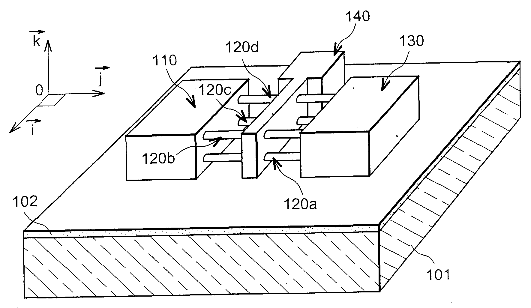
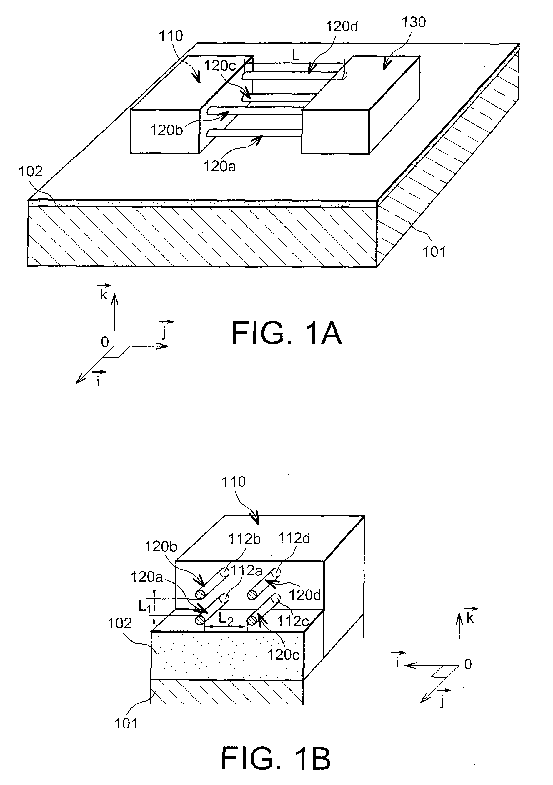
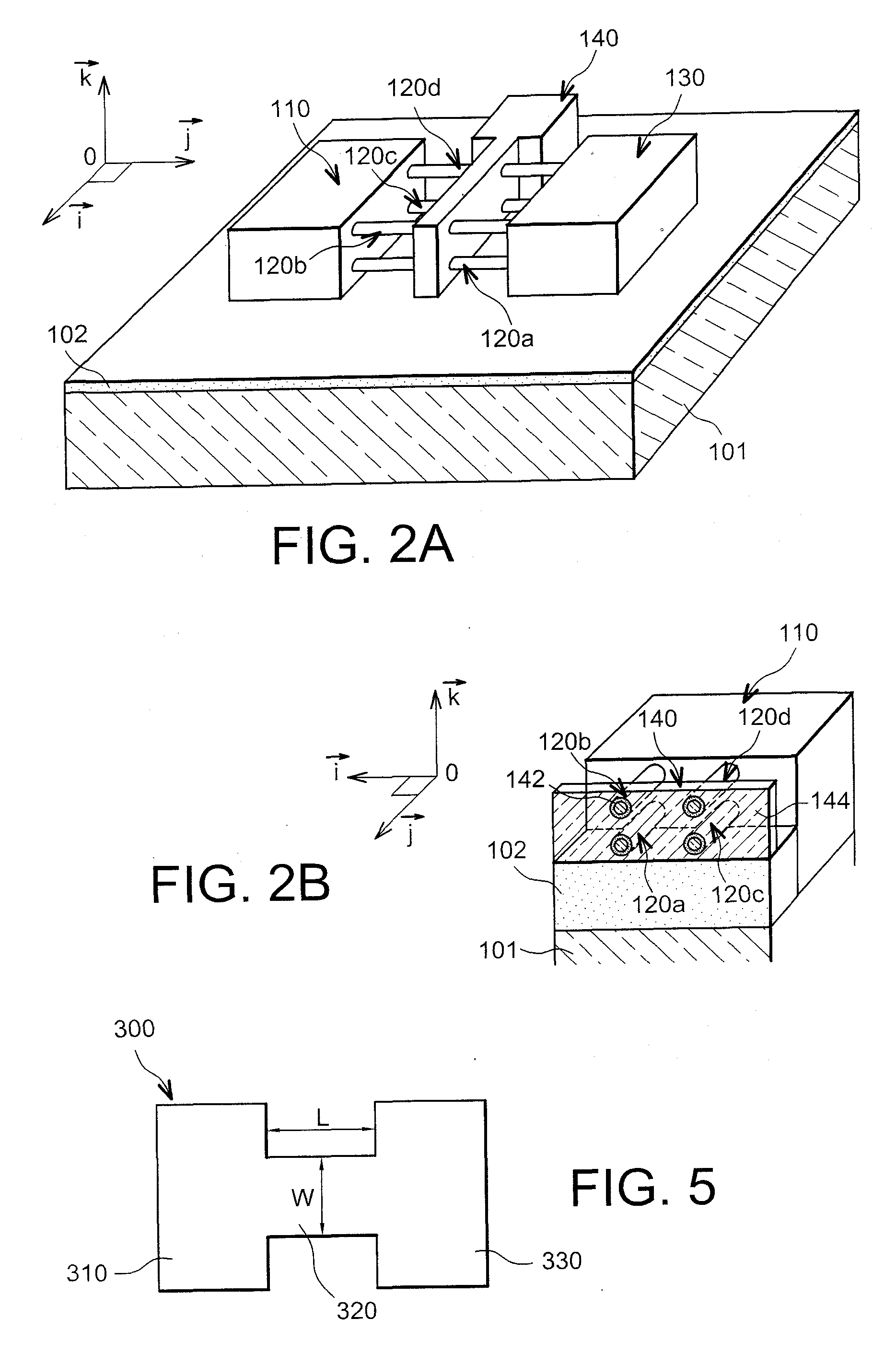
[0009]The object of the present invention is to present a field effect microelectronic device comprising one or more wires, called > wires, that are optimized in terms of arrangement, shape or / and composition, and are able to form an improved transistor channel, or channel with several branches, or several transistor channels. These wires, forming one or more transistor channels, have an arrangement, and a shape or / and a composition bringing improvements to field effect transistors, in particular in terms of integration density and electrical performance.

[0010]The invention also provides a method for fabricating a microelectronic device having one or more bars or rods or wires, called > able to form a transistor channel or a transistor channel with several branches or several transistor channels, the method comprising the steps of:

[0011]a) the forming, in one or more thin layers, of at least one first block and at least one second block in which respectively at least one transistor ...


PUM


Abstract

A microelectronic device provided with one or more quantum wires, able to form one or more transistor channels, and optimized in terms of arrangement, shape, and/or composition. A method for fabricating the device includes forming, in one or more thin layers resting on a support, a first block and a second block in which at least one transistor drain region and at least one transistor source region are respectively intended to be formed, forming a structure connecting the first block to the second block, and forming, on the surface of the structure, wires connecting a first region of the first block with another region of the second block that faces the first region.

Description

TECHNICAL AREA[0001]The present invention relates to the field of integrated circuits and more specifically to the field of transistors, and its objective is to present a microelectronic device provided in particular with one or more quantum wires that are optimized in terms of arrangement, shape or / and composition, and able to form a transistor channel, a transistor channel with several branches, or several transistor channels having improved electric performance and bulkiness.PRIOR ART[0002]A conventional transistor structure formed on a substrate, e.g. of SOI type (<<Silicon On Insulator>>), generally consists of a source region and drain region in the form for example of respective first and second semiconductor regions, joined together by a third semiconductor region or channel which may be in the shape of a bar or parallelepiped block. This bar is coated with a gate enabling control over the intensity of a current transiting between the source region and the drain ...

Claims


Application Information

Patent Timeline
IPC IPC(8): H01L29/12H01L21/336
CPCB82Y10/00H01L29/78696H01L29/775H01L29/42392
Inventor ERNST, THOMASBOREL, STEPHAN
Owner COMMISSARIAT A LENERGIE ATOMIQUE ET AUX ENERGIES ALTERNATIVES
Why Eureka
Try Eureka