Floating body memory cell having gates favoring different conductivity type regions

a floating body memory and gate technology, applied in the direction of semiconductor devices, electrical equipment, transistors, etc., can solve the problems of low efficiency, difficult to fabricate structures, and relative high voltage required on the back ga

Active Publication Date: 2008-06-26
INTEL CORP
View PDF32 Cites 142 Cited by
  • Summary
  • Abstract
  • Description
  • Claims
  • Application Information

AI Technical Summary

Problems solved by technology

One problem with this arrangement is the relatively high voltage required on the back gate because of the thick oxide.
As the oxide is thinned, the gate leakage becomes high, causing the tunneling of electrons, which has the effect of erasing the stored charge.
These...

Method used


Image

  • Floating body memory cell having gates favoring different conductivity type regions
  • Floating body memory cell having gates favoring different conductivity type regions
  • Floating body memory cell having gates favoring different conductivity type regions

Examples


Embodiment Construction

[0040]In the following description, a memory and method for fabricating the memory is described. Numerous specific details are set forth, such as specific conductivity types, to provide a thorough understanding of the present invention. It will be apparent to one skilled in the art, that the present invention may be practiced without these specific details. In other instances, well known processing steps and circuits have not been described in detail, in order not to unnecessarily obscure the present invention.

Floating Body Cell Operation and Prior Art Devices

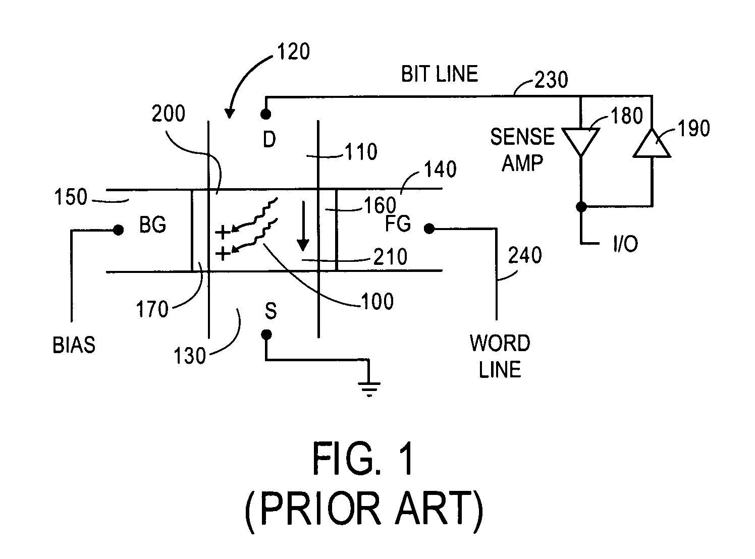
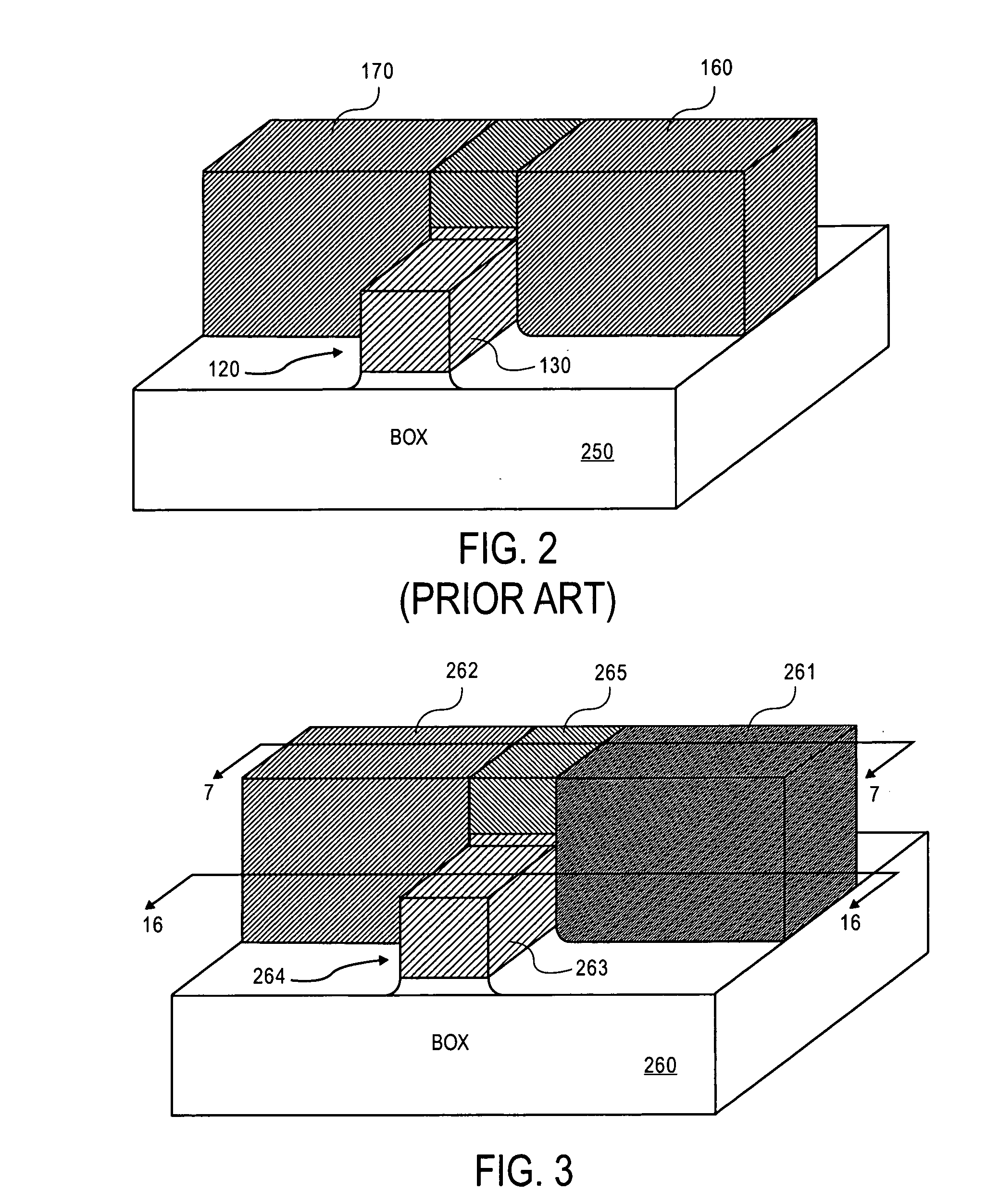
[0041]A single memory cell is shown in schematic form in FIG. 1. A portion of a semiconductor line, body or fin 120, formed on an oxide layer (such as BOX 250 of FIG. 2), and etched from, for example, a monocrystalline silicon layer is illustrated. The body 120 includes a pair of spaced-apart, doped regions 110 and 130, disposed at opposite ends of the body thereby defining a channel region 100. In one embodiment, the channel r...


PUM


Abstract

A method for fabricating floating body memory cells (FBCs), and the resultant FBCs where gates favoring different conductivity type regions are used is described. In one embodiment, a p type back gate with a thicker insulation is used with a thinner insulated n type front gate. Processing, which compensates for misalignment, which allows the different oxide and gate materials to be fabricated is described.

Description

FIELD OF THE INVENTION[0001]This invention relates to the field of dynamic, random-access memories (DRAMs), and devices with double gates, particularly those using transistors with floating bodies, also known as floating body cells (FBCs).PRIOR ART AND RELATED ART[0002]Most common DRAM cells store charge on a capacitor and use a single transistor for accessing the capacitor. More recently, a cell has been proposed which stores charge in a floating body of a transistor. A back gate is biased to retain charge in the floating body.[0003]In one proposal, an oxide layer is formed on a silicon substrate and a silicon layer for the active devices is formed on the oxide layer (SOI substrate). The floating bodies are defined from the silicon layer and the substrate is used as a back or biased gate. One problem with this arrangement is the relatively high voltage required on the back gate because of the thick oxide. For this structure and others, when FBCs are scaled to state-of-the-art gate ...

Claims


Application Information

Patent Timeline
IPC IPC(8): H01L27/108H01L21/8242
CPCH01L27/108H01L27/10802H01L27/10826H01L27/10879H01L29/78H01L29/7841H01L29/785Y10S257/903H01L29/66477H01L27/1203H10B12/20H10B12/36H10B12/056H10B12/00H10B99/00H10B12/01H01L21/28008H01L29/66795H01L29/7851H01L21/823821H01L21/823828H01L21/823857H01L21/823878H01L27/0924H01L29/0649H01L29/495H01L29/4966H01L29/51H01L21/823892H01L27/0928H01L29/0653H01L29/16H01L29/517
Inventor CHANG, PETER L.D.AVCI, UYGAR E.KENCKE, DAVID L.BAN, IBRAHIM
Owner INTEL CORP
Why Eureka
Try Eureka