Spin transfer MRAM device with magnetic biasing

a magnetic biasing and transfer mram technology, applied in the field of magnetic memories, can solve the problems of increasing the current required to generate the necessary magnetic field, the disturbance of the cell that shares the same word line or bit line, and the difficulty in maintaining the needed level of electric current, so as to achieve the effect of significant power saving and tight control of the current puls

Active Publication Date: 2008-06-26
TAIWAN SEMICON MFG CO LTD
View PDF13 Cites 128 Cited by
  • Summary
  • Abstract
  • Description
  • Claims
  • Application Information

AI Technical Summary

Benefits of technology

[0027]This overcomes the problem of very tight control of the current pulse in a conventional device based on spin-transfer induced switching. This scheme may be further refined by adopting a segmented word line layout in which the write word line current is applied to a limited number of devices (on a shared word line) while spin currents are applied for each individual bit to write into their desired magnetic states. This is associated with significant power saving since multiple bits share the same word write line.

Problems solved by technology

The problem of keeping cells that share the same word line or bit line being disturbed is a major concern.
As the device is further microminiarurized, the address wiring is reduced in width so that it becomes difficult to sustain the needed level of electric current.
Furthermore, since the coercive force of the device is also increased, the current required to generate the necessary magnetic field, and hence the power consumption, is also increased.
This may result in a reversal of the magnetic moment vector along its easy axis.
Maintaining magnetization in a direction normal to the plane of a disk is, in general, difficult to achieve.
It is anticipated that maintaining such accuracy in the definition of the current pulse might prove to be extremely problematic, largely due to varying sources of impedance.
Also the current density required for spin-torque switching is too large for ready integration with CMOS technology.

Method used


Image

  • Spin transfer MRAM device with magnetic biasing
  • Spin transfer MRAM device with magnetic biasing
  • Spin transfer MRAM device with magnetic biasing

Examples


Embodiment Construction

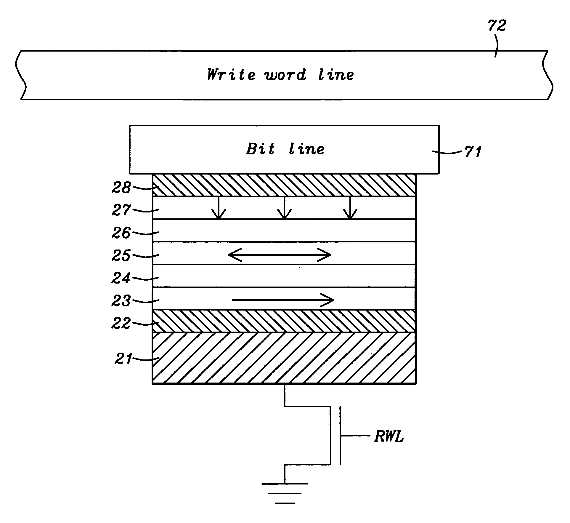
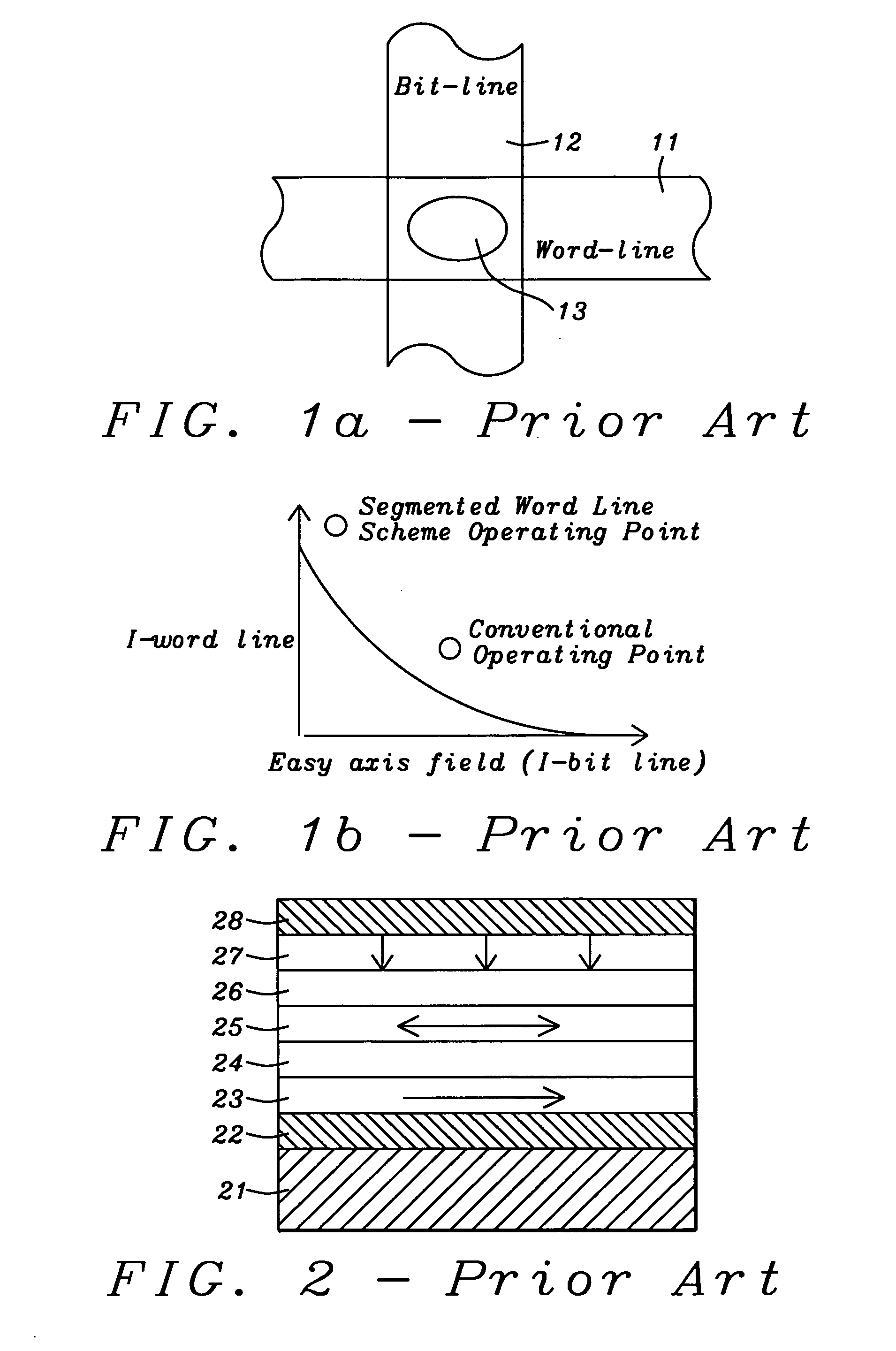
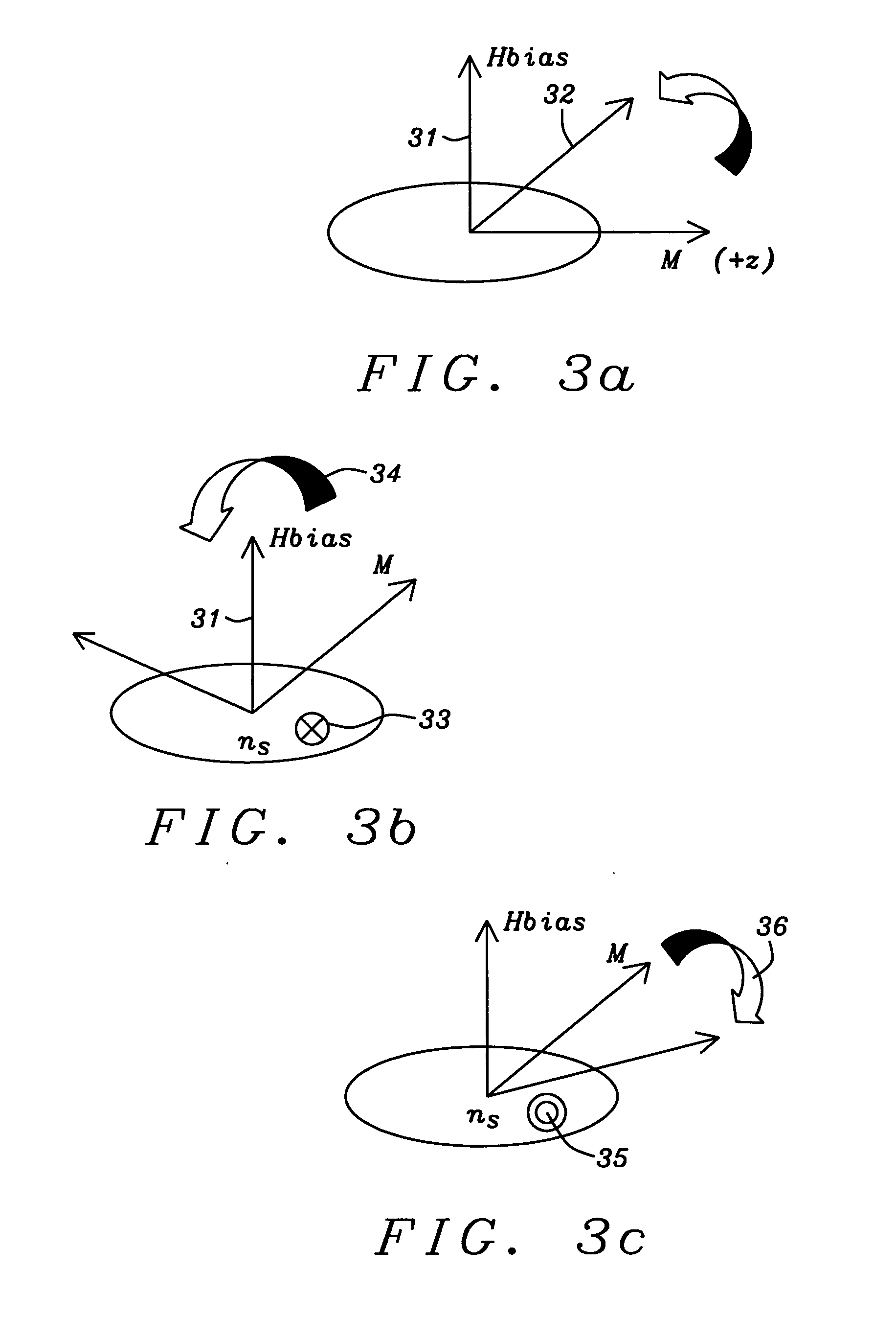
[0036]To solve the problems outlined in the earlier section, the present invention discloses a hybrid MRAM structure that combines spin-transfer with magnetic biasing. As shown in FIG. 3a, the electric current flowing in a write word line generates a magnetic field 31 to bias the magnetization 32 of the free layer toward its hard axis.

[0037]It is shown in FIG. 3b that, when spin direction 33 is into the paper the spin current generates torque 34 to help switch the magnetization of the free layer. As seen in FIG. 3c, when spin direction 35 is out of the paper, the spin current generated torque 36 only balances the bias field, rotating the free layer magnetization back towards its original easy axis direction.

[0038]Thus, the torque on the free layer magnetization is dependent upon the spin direction, which is in turn determined by the current flow direction and the magnetization of the drive layer. When electrons flow from drive layer to free layer, the current carries spins polarized...


PUM


Abstract

The addition of segmented write word lines to a spin-transfer MRAM structure serves to magnetically bias the free layer so that the precessional motion of the magnetization vector that is set in play by the flow of spin polarized electrons into the free layer allows said magnetic vector to be switched rather than to oscillate between two easy axis directions.

Description

FIELD OF THE INVENTION[0001]The invention relates to the general field of magnetic memories with particular reference to improving spin polarization in devices based on this.BACKGROUND OF THE INVENTION[0002]Magnetic random access memories (MRAMs) using magnetic tunneling junctions (MTJs) are strong candidates to provide a dense (area=˜8-25 f2, where f is the smallest feature size), fast (1˜30 ns read / write speed), and non-volatile storage solution for future memory applications. The MTJ utilizes at least two magnetic layers that sandwich a thin dielectric insulting layer such as Al2O3, AlNxOy, or MgO, with one magnetic layer pinned by an anti-ferromagnetic film. To protect data from erasure or thermal agitation, an in-plane uniaxial magnetic anisotropy is needed for the magnetic free layer to store data.[0003]As seen in FIG. 1a, the cross point of Word Line 11 and Bit Line 12 currents programs MTJ cell 13. The problem of keeping cells that share the same word line or bit line being ...

Claims


Application Information

Patent Timeline
Patent Type & Authority Applications(United States)
IPC IPC(8): G11C11/00H01L29/82H01L21/00
CPCG11C11/16G11C11/1675G11C11/161
Inventor GUO, YIMIN
Owner TAIWAN SEMICON MFG CO LTD
Why Eureka
Try Eureka