
Method for fabricating flash memory device

a technology of flash memory and fabrication method, which is applied in the direction of semiconductor devices, basic electric elements, electrical apparatus, etc., can solve the problems of unstable program/erase characteristics of sonos devices, inability to shrunk past a certain level, and inability to use devices as memory devices, etc., to achieve the effect of stabilizing the electrical properties of sonos devices and easy infiltrating ono layers

Inactive Publication Date: 2008-06-26
DONGBU HITEK CO LTD
View PDF8 Cites 2 Cited by
  • Summary
  • Abstract
  • Description
  • Claims
  • Application Information

AI Technical Summary

Benefits of technology

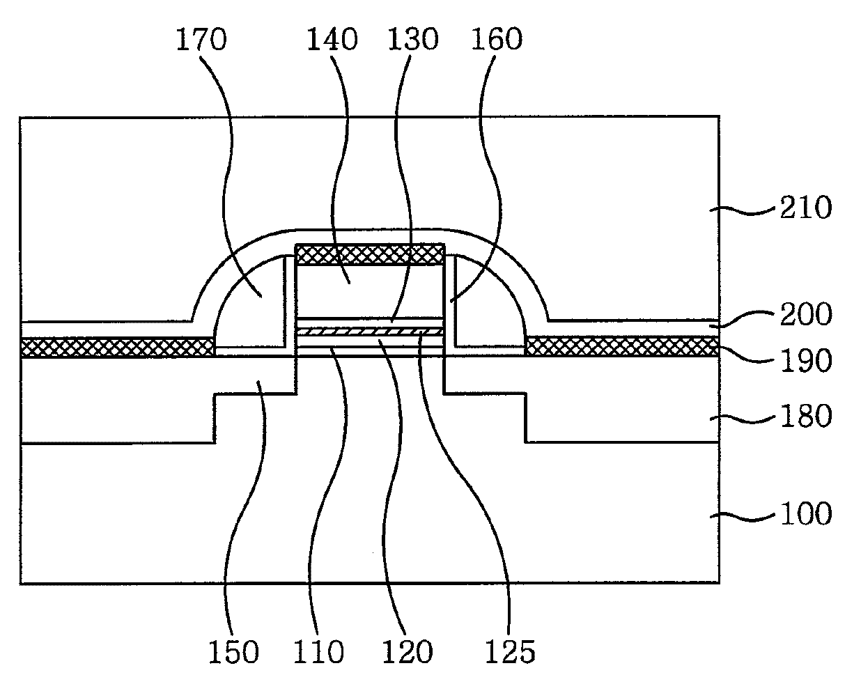
[0022]In general, example embodiments of the invention relate to a method for fabricating flash memory devices in which hydrogen can easily infiltrate an ONO layer of a SONOS device and a probability of the infiltrated hydrogen being combined with dangling bonds, shallow traps, and / or interface traps is increased, thereby stabilizing the electrical properties of the SONOS device.
[0023]Example embodiments of the invention also relate to a method for fabricating flash memory devices in which a threshold voltage window is widened due to stabilized program / erase characteristics of a SONOS device, improving the yield and reliability of the flash memory devices.

Problems solved by technology

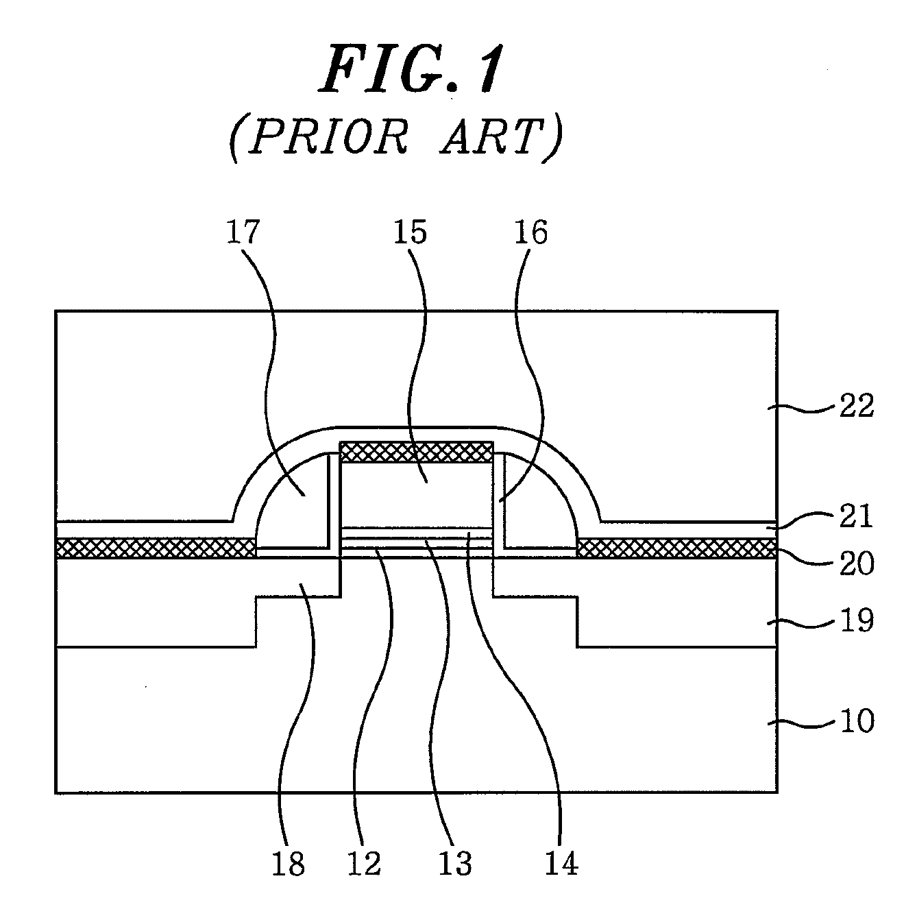
However, the conventional floating gate cell requires a high voltage upon program / erasure and therefore cannot be shrunk past a certain level.
This incomplete interface makes the program / erase characteristics of the SONOS device unstable, e.g., reducing a threshold voltage (Vt) window.
This makes it impossible to use the device as a memory device.
Further, a retention characteristic (that is, a charge retention ability) and a durability characteristic (that is, a read and write ability) are depreciated, lowering reliability of the device.
In the fabrication method of the SONOS device, it is difficult to raise the temperature of the sintering process to 435° C. or more.
Accordingly, not only it is difficult to infiltrate hydrogen into the ONO layer of the SONOS device, but also a probability of the infiltrated hydrogen being combined with dangling bonds, shallow traps and / or interface traps is lowered.
Consequently, the stabilization of electrical properties of the SONOS device, such as program and erase characteristics, retention ability, and durability, is limited.

Method used


Image

  • Method for fabricating flash memory device
  • Method for fabricating flash memory device
  • Method for fabricating flash memory device

Examples


Embodiment Construction

[0022]In general, example embodiments of the invention relate to a method for fabricating flash memory devices in which hydrogen can easily infiltrate an ONO layer of a SONOS device and a probability of the infiltrated hydrogen being combined with dangling bonds, shallow traps, and / or interface traps is increased, thereby stabilizing the electrical properties of the SONOS device.

[0023]Example embodiments of the invention also relate to a method for fabricating flash memory devices in which a threshold voltage window is widened due to stabilized program / erase characteristics of a SONOS device, improving the yield and reliability of the flash memory devices.

[0024]In accordance with example embodiments, there is provided a method for fabricating a flash memory device, including the steps of forming an ONO layer over a semiconductor substrate, forming a gate electrode on the ONO layer, forming a source / drain impurity region in a surface of the semiconductor substrate on both sides of th...


PUM

PropertyMeasurementUnit
temperatureaaaaaaaaaa

Abstract

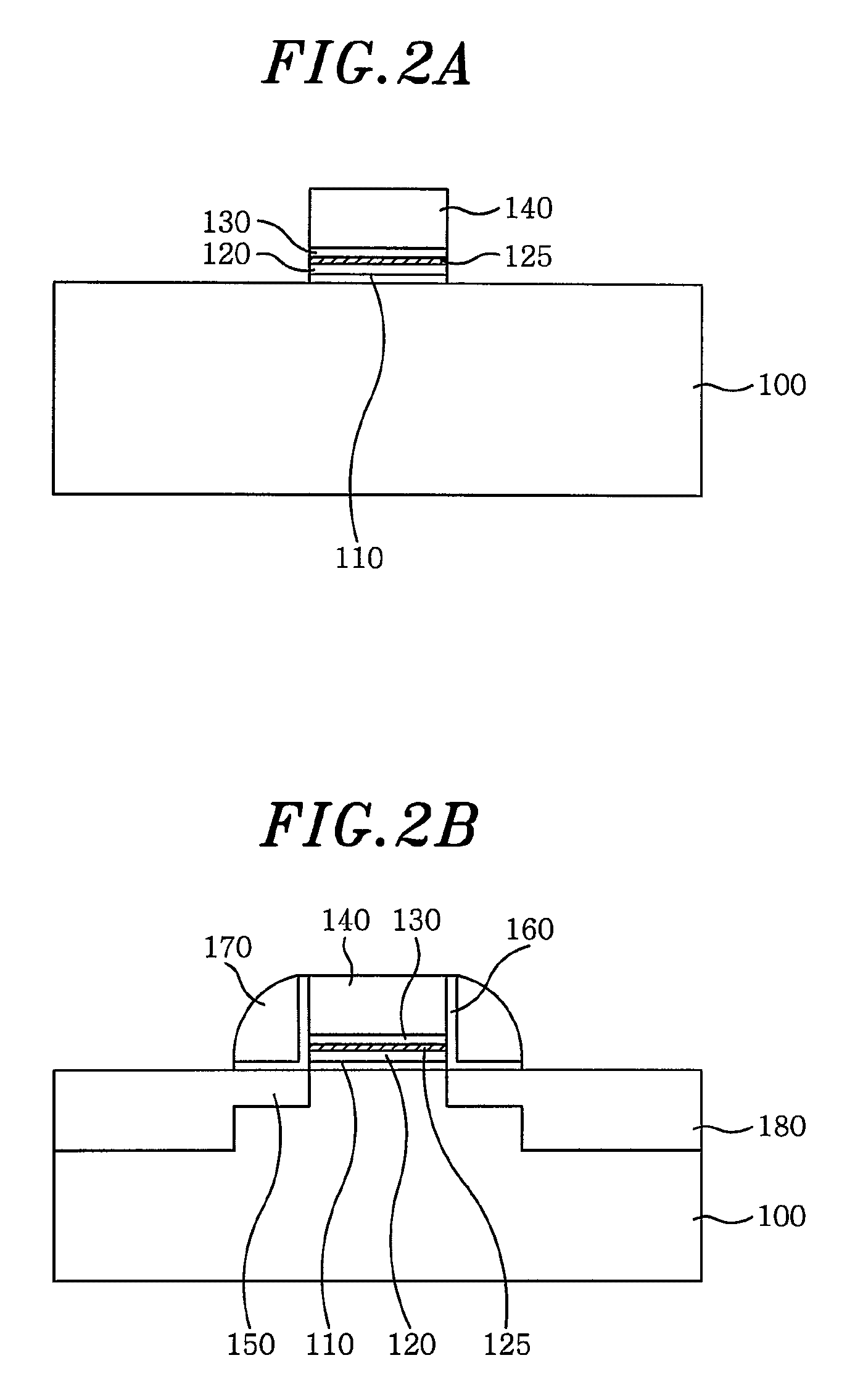
The present invention relates to a method for fabricating flash memory devices. The method may include the steps of forming an oxide / nitride / oxide (ONO) layer over a semiconductor substrate and a gate electrode on the ONO layer. Next, source / drain impurity region may be formed in a surface of the semiconductor substrate on both sides of the gate electrode and a pre-metal dielectric (PMD) layer may be formed over an entire surface of the semiconductor substrate including the gate electrode. Finally, a densification process for densifying the PMD layer may be performed under a gas atmosphere. A densification gas atmosphere used for densifying the PMD layer may include an H2 or N2 / H2 atmosphere.

Description

CROSS-REFERENCE TO RELATED APPLICATION[0001]This application claims priority to Korean Application No. 10-2006-0132345, filed on Dec. 22, 2006, and to Korean Application No. 10-2006-0133260, filed on Dec. 23, 2006, each of which are incorporated herein by reference in their entirety.BACKGROUND[0002]1. Field of the Invention[0003]The present invention relates to a method for fabricating flash memory devices.[0004]2. Background of the Invention[0005]In general, a representative example of a flash memory device, that is, a non-volatile memory device whose data is not lost even when power is not supplied to the device, includes electrically erasable and programmable read only memory (EEPROM).[0006]EEPROM is an electrically rewritable non-volatile memory device and generally has a structure employing a stacked floating-gate cell.[0007]In recent years, as the level of integration rapidly increases, there is an urgent need for a reduction in size of the conventional floating gate cell. How...

Claims


Application Information

Patent Timeline
Patent Type & Authority Applications(United States)
IPC IPC(8): H01L21/336
CPCH01L21/28282H01L21/76828H01L21/76826H01L21/3105H01L29/40117
Inventor JEONG, DAE HO
Owner DONGBU HITEK CO LTD
Learn More