Power Semiconductor Device

a technology of semiconductor devices and power semiconductors, applied in the field of power semiconductor devices, can solve the problems of reducing the active region of the avalanche break-down voltage, increasing the miller capacitance and reducing the switching speed, and erroneous operation easily occurring, so as to reduce the number of gate bus lines, improve the flow of source current, and reduce the area loss

Inactive Publication Date: 2008-07-03
KEC
View PDF5 Cites 2 Cited by
  • Summary
  • Abstract
  • Description
  • Claims
  • Application Information

AI Technical Summary

Benefits of technology

[0032]Since the gate polysilicon extends between the respective first conductive regions along an approximately S-shaped p

Problems solved by technology

The closed-cell-type semiconductor device has a problem in that, since the junctions between the P type first conductive regions 130′ and the N type epitaxial layer 120′ have a shape similar to that of a spherical surface, Avalanche break-down voltage decreases in the active region.
This increases Miller capacitance and decreases switching speed.
When

Method used


Image

  • Power Semiconductor Device
  • Power Semiconductor Device
  • Power Semiconductor Device

Examples


Embodiment Construction

[0051]Reference will now be made in detail to the preferred embodiments of the present invention.

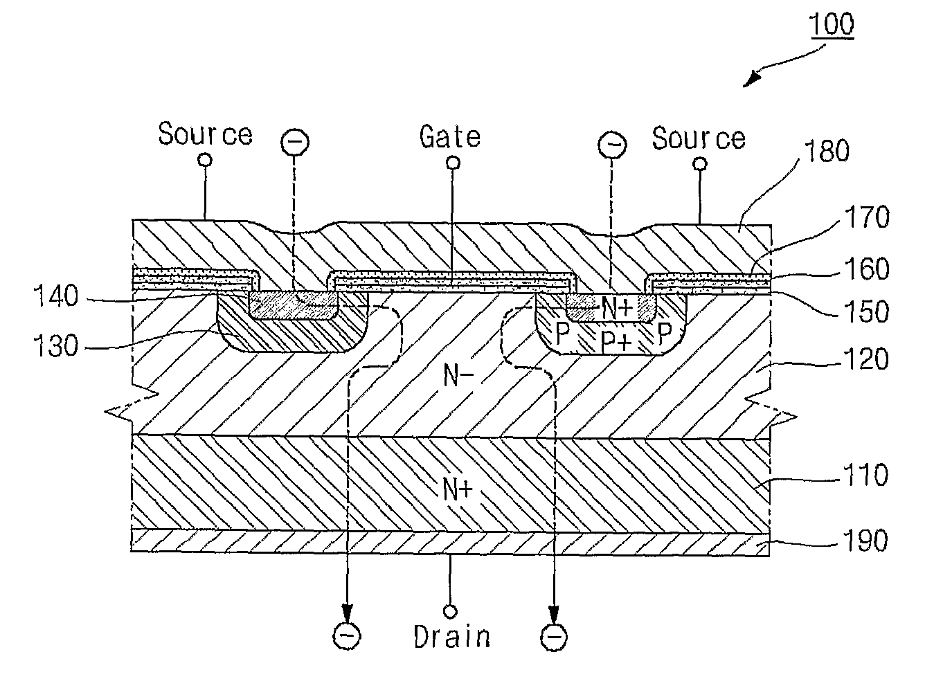
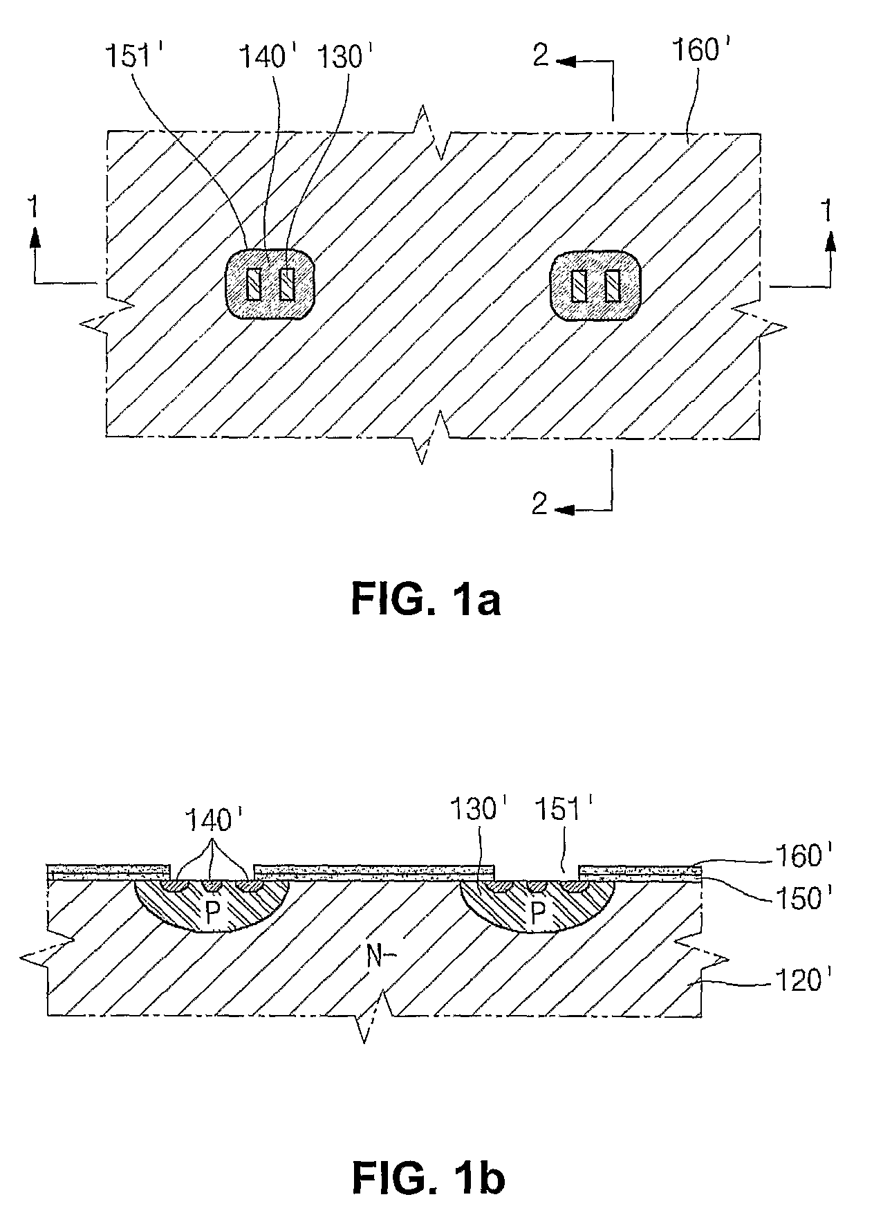
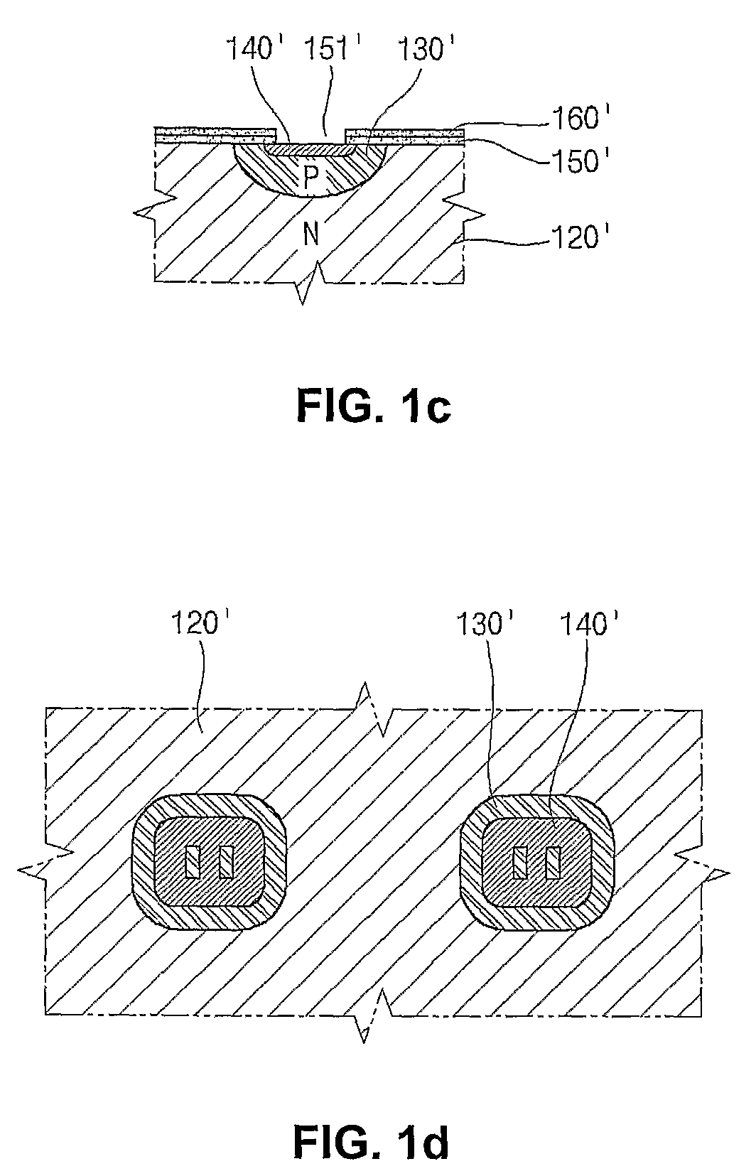
[0052]Referring to FIG. 3a, a partial top view showing a power semiconductor device according to the present invention is illustrated; referring to FIG. 3b, a sectional view taken along line 5-5 of FIG. 3a is illustrated; referring to FIG. 3c, a sectional view taken along line 6-6 of FIG. 3a is illustrated; and, referring to FIG. 3d, a top view showing only the top portion of the semiconductor device shown in FIG. 3a is illustrated.

[0053]As shown, the power semiconductor device 100 according to the present invention includes an epitaxial layer 120, a number of first conductive regions 130 formed on the surface of the epitaxial layer 120 with a predetermined spacing; second conductive regions 140 formed in the respective first conductive regions 130; gate oxide 150 formed on the surface of the epitaxial layer 120 in such a manner that a window is provided in each first conductive region 1...


PUM


Abstract

Disclosed is a power semiconductor device capable of transmitting a gate signal from any upward, downward, leftward, and rightward directions on a plane to reduce deviation in the gate signal's transmission speed and impedance. The power semiconductor device includes a conductive low-density epitaxial layer; a first conductive region having a number of first conductive layers formed linearly on the surface of the epitaxial layer with predetermined spacing and depth and a number of second conductive layers formed linearly with a predetermined spacing while being spaced a predetermined distance from ends of the first conductive >layers; a second conducive region formed with a width and a depth smaller than those of the first and second conductive layers so that channels can be formed on the first and second conductive layers, respectively; gate oxide having a first window formed on the surface of the epitaxial layer with a width smaller than that of the first conductive layers and a second window formed with a width smaller than that of the second conductive layers; and gate polysilicon formed on the gate oxide.

Description

TECHNICAL FIELD[0001]The present invention relates to a power semiconductor device, and more particularly to a power semiconductor device capable of transmitting a gate signal from any upward, downward, leftward, and rightward directions on a plane to reduce deviation in the gate signal's transmission speed and impedance.BACKGROUND ART[0002]In general, power semiconductor devices (for example, power MOSFETs or IGBTs) are manufactured in a trench or planar type. Planar-type power semiconductor devices are used for switching-mode power supplies, DC-DC converters, electronic stabilizers for fluorescent lamps, and inverters for motors. They need to have small switching loss and conduction loss and sufficiently high yield voltage. By using these devices, it is possible to reduce the size of final products due to increased energy efficiency and decreased heat. The planar-type power semiconductor devices are classified into closed-cell-type devices and stripe-type devices.[0003]As shown in...

Claims


Application Information

Patent Timeline
IPC IPC(8): H01L29/78
CPCH01L29/0696H01L29/7802H01L29/7395H01L29/0852
Inventor LEE, YOUNG WONCHO, MOON SOO
Owner KEC
Why Eureka
Try Eureka