Gate structure

a technology of gate structure and dielectric layer, which is applied in the direction of basic electric elements, electrical apparatus, and semiconductor devices, can solve the problems of high-k dielectric layer, rapid increase of leakage current, and drop in mobility and device reliability, and achieve the effect of increasing device performan

Inactive Publication Date: 2008-07-03
UNITED MICROELECTRONICS CORP
View PDF6 Cites 13 Cited by
  • Summary
  • Abstract
  • Description
  • Claims
  • Application Information

AI Technical Summary

Benefits of technology

[0008]Accordingly, at least one objective of the present invention is to provide a method of fabricating a gate structure that can prevent the problem of having inferior properties at the interface between a high K (dielectric constant) dielectric layer and a substrate and increase device performance.
[0009]At least another objective of the present invention is to provide a gate structure that can resolve the problem of having inferior properties at the interface between a high K dielectric layer and a substrate.
[0022]In the present invention, the method of forming a sacrificial oxide layer and then removing it in a subsequent process is used to prevent the surface of the interface layer from receiving any damages so that the quality of the film layer is improved. Furthermore, because the area with a high concentration of nitrogen atoms can be removed leading to a lower concentration of nitrogen in the substrate after removing the sacrificial oxide layer, the concentration profile of the nitrogen is better control and prevents the reduction of electron mobility. Moreover, with the reduction in the concentration of nitrogen in the substrate, the concentration of nitrogen in the interface layer is lower so that the equivalent oxide thickness (EOT) is reduced. Ultimately, the performance of the device is improved.

Problems solved by technology

As a result, the chance of having a direct tunneling will increase leading to a rapid increase in the leakage current.
However, the integration of a high-K dielectric layer with transistors often encounters some technical difficulties because the use of a high-K material often results in a drop in mobility and device reliability.
However, the effect of polysilicon gate depletion can hardly be avoided.
Furthermore, the deployment of a high-K dielectric layer tends to increase the threshold voltage of a device and prevents the integration of the high-K dielectric layer with a polysilicon gate.

Method used


Image

  • Gate structure
  • Gate structure
  • Gate structure

Examples


Embodiment Construction

[0027]Reference will now be made in detail to the present preferred embodiments of the invention, examples of which are illustrated in the accompanying drawings. Wherever possible, the same reference numbers are used in the drawings and the description to refer to the same or like parts.

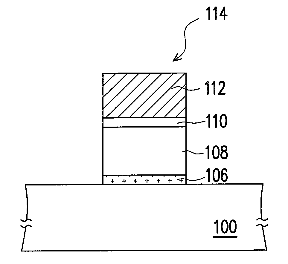
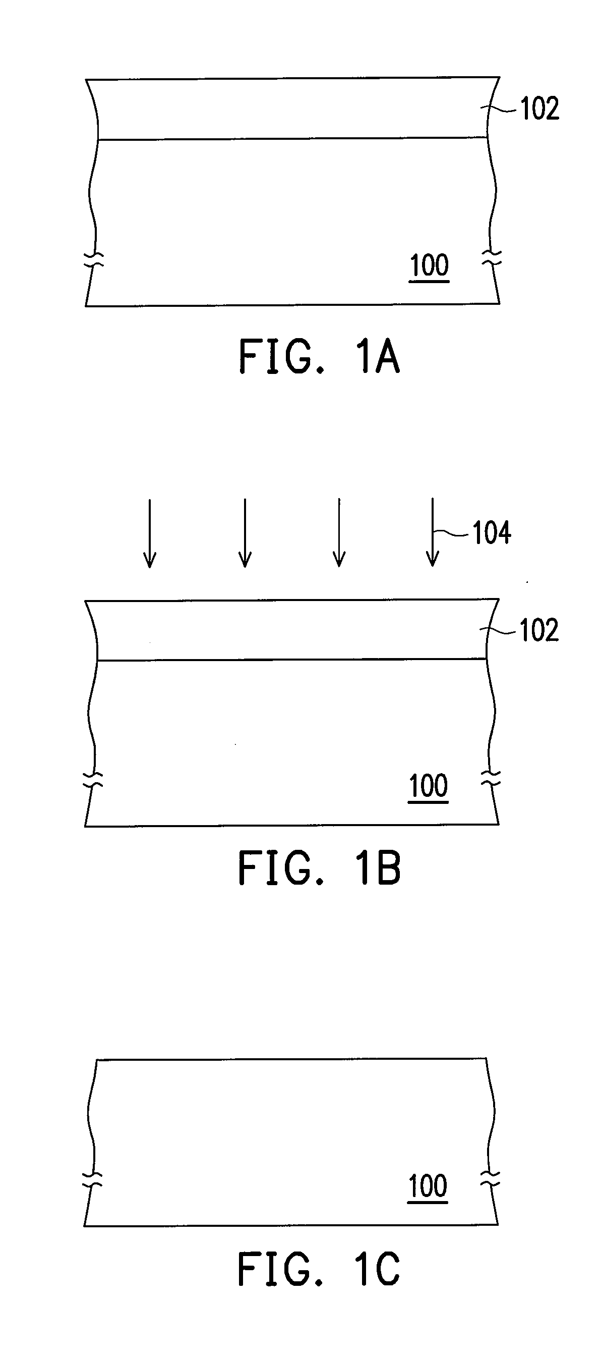
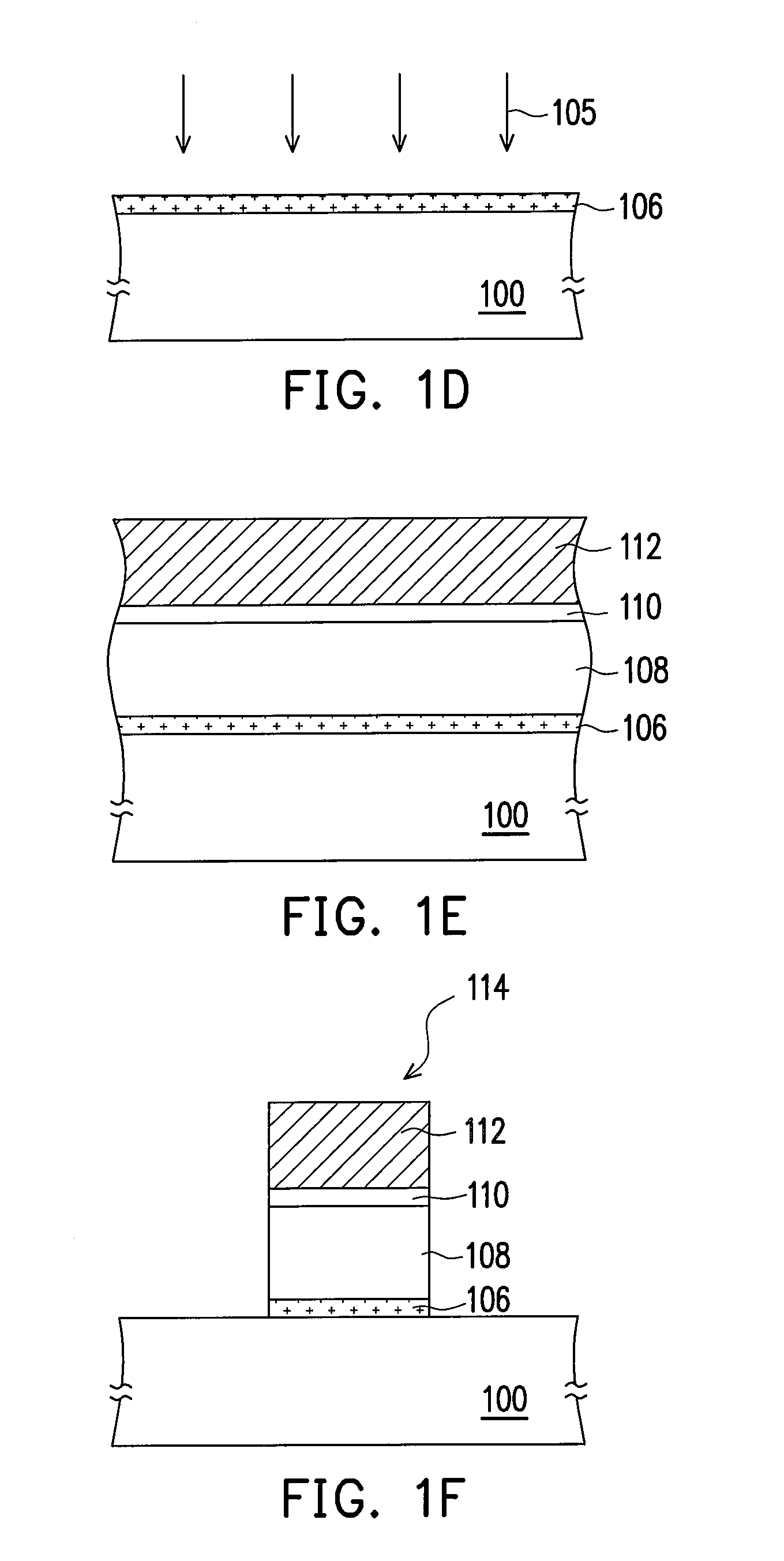
[0028]The method of fabricating a gate structure in the present invention includes forming an interface layer between a high dielectric constant (high-K) dielectric layer and a silicon substrate so that the problem of having inferior properties at the interface between a high-K dielectric layer and a silicon substrate is resolved. The conventional method includes forming an oxide layer over the silicon substrate and performing a plasma process to form the interface layer. As a result, the plasma may damage the surface of the interface layer and the oxide layer may re-grow. In another conventional method, a plasma nitridation process is performed before performing a re-oxidation process to form the af...


PUM


Abstract

A method of fabricating a gate structure is provided. First, a sacrificial oxide layer is formed on a substrate. A nitridation treatment process is performed to redistribute the nitrogen atoms in the sacrificial layer and the substrate and produce a concentration profile such that the concentration of nitrogen progressively increases and then decreases toward the substrate with the maximum concentration of nitrogen in the sacrificial oxide layer. Next, the sacrificial oxide layer is removed. A re-oxidation process is performed to produce an interface layer on the surface of the substrate. A high K (dielectric constant) gate dielectric layer, a barrier layer and a metal layer are sequentially formed on the substrate. The metal layer, the barrier layer, the high K gate dielectric layer and the interface layer are defined to form a stacked gate structure.

Description

CROSS-REFERENCE TO RELATED APPLICATION[0001]This application is a divisional of an application Ser. No. 11 / 164,025, filed on Nov. 8, 2005, now pending. The entirety of the above-mentioned patent application is hereby incorporated by reference herein and made a part of this specification.BACKGROUND OF THE INVENTION[0002]1. Field of the Invention[0003]The present invention relates to a semiconductor process. More particularly, the present invention relates to a gate structure and a method of fabricating the same.[0004]2. Description of the Related Art[0005]In most conventional semiconductor process, silicon oxide (SiO2) is used to form the gate dielectric layer. With the rapid progress in the integrated circuit manufacturing industry, the design of circuit devices increasingly depends on miniaturization to increase the level of device integration and the driving capability of the devices. As the line width of gates is reduced, thickness of the gate dielectric layer must be reduced cor...

Claims


Application Information

Patent Timeline
Patent Type & Authority Applications(United States)
IPC IPC(8): H01L29/94
CPCH01L21/28088H01L21/28202H01L29/518H01L29/4966H01L29/517H01L21/76822
Inventor WANG, YUN-RENYEN, YING-WEICHAN, SHU-YENHUANG, KUO-TAI
Owner UNITED MICROELECTRONICS CORP
Why Eureka
Try Eureka