Chip package structure

Inactive Publication Date: 2008-07-03
CHIPMOS TECH INC
View PDF2 Cites 1 Cited by
  • Summary
  • Abstract
  • Description
  • Claims
  • Application Information

AI Technical Summary

Benefits of technology

[0009]A chip package structure which reduces the volume of the

Problems solved by technology

Therefore, the length of the third bonding wires 150 is longer, which renders the third bonding wires 150 prone to collapse and thereby causing electric short circui

Method used


Image

  • Chip package structure
  • Chip package structure
  • Chip package structure

Examples


first embodiment

The First Embodiment

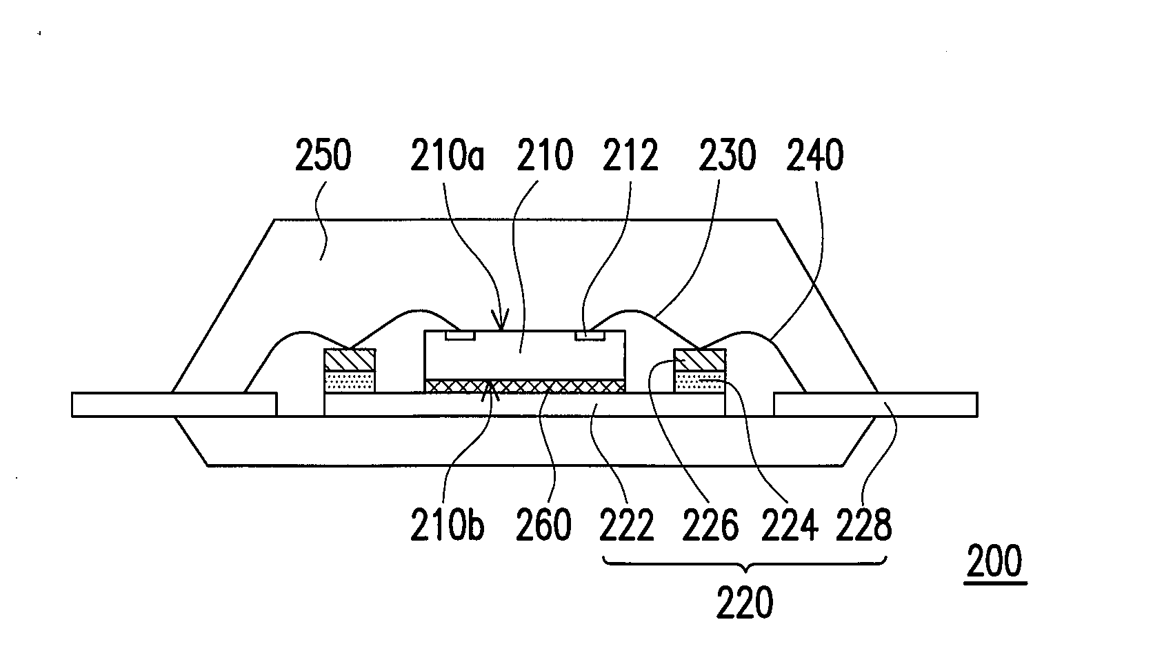
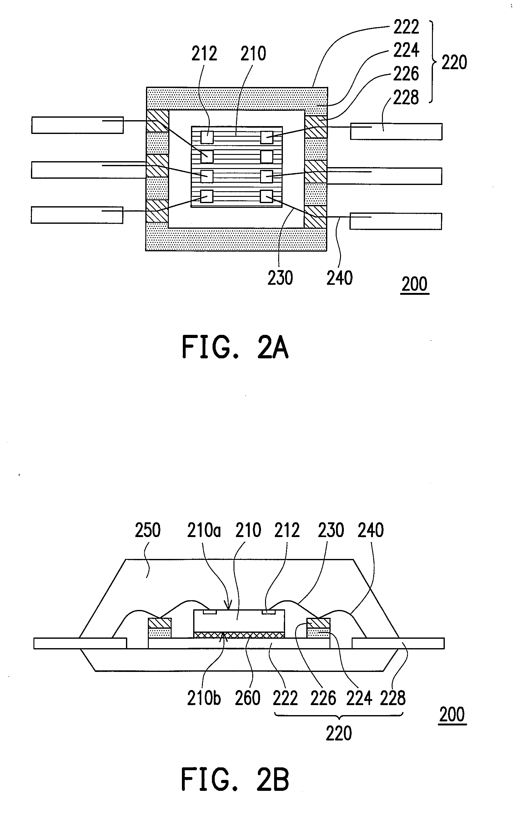
[0024]FIG. 2A is a schematic cross-sectional side view of the chip package structure according to the first embodiment of the present invention. FIG. 2B is a schematic top view of the lead frame of the chip package structure in FIG. 2A. Referring to both FIGS. 2A and 2B, a chip package structure 200 of the first embodiment includes a chip 210, a lead frame 220, a plurality of first bonding wires 230 and a plurality of second bonding wires 240. The chip 210 has an active surface 210a, a back surface 210b and a plurality of bonding pads 212. The bonding pads 212 disposed on the active surface 210a of the chip 210 may be ground bonding pads, power bonding pads or signal bonding pads. Additionally, the bonding pads 212 are usually disposed on the edge of the chip 210 so as to facilitate the wire bonding process.

[0025]The lead frame 220 includes a die pad 222, an insulating layer 224, a plurality of transfer bonding pads 226 and a plurality of inner leads 228. The bac...

second embodiment

The Second Embodiment

[0028]FIG. 4 is a schematic top view of the chip package structure according to the second embodiment of the invention. Referring to FIG. 4, a chip package structure 200′″ has a structure approximately identical to that of the chip package structure 200 in FIG. 2A. The difference between them is that the chip package structure 200′″ has a plurality of insulating pads 224′″ that are separate from one another and the transfer bonding pads 226 are respectively disposed on the insulating pads 224′″. The other elements of the chip package structure 200′″ are approximately identical to those of the chip package structure 200 in FIG. 2A. Thus, they are not to be reiterated herein.

[0029]In the chip package structure of the invention, the insulating layer (or insulating pads) and the transfer bonding pads disposed on the die pad are used to integrate the bus bar in the lead frame into the die pad so that the overall volume of the chip package structure is reduced.

[0030]B...


PUM


Abstract

A chip package structure including a chip, a lead frame, first bonding wires and second bonding wires is provided. The chip has an active surface, a back surface and bonding pads disposed on the active surface. The lead frame includes a die pad, an insulating layer, transfer bonding pads and inner leads. The back surface of the chip is fixed on the die pad. The insulating layer is disposed on the die pad outside the chip. The transfer bonding pads are disposed on the insulating layer. The first bonding wires are respectively connected to the bonding pads and the transfer bonding pads. The second bonding wires are respectively connected to the transfer bonding pads and the inner leads. The chip package structure has smaller volume and a higher yield rate.

Description

CROSS-REFERENCE TO RELATED APPLICATION[0001]This application claims the priority benefit of P.R.C. application serial no. 200610172822.3, filed Dec. 29, 2006. All disclosure of the P.R.C. application is incorporated herein by reference.BACKGROUND OF THE INVENTION[0002]1. Field of the Invention[0003]The present invention relates to a semiconductor device and a fabricating method thereof. More specifically, the invention relates to a chip package structure and a fabricating method thereof.[0004]2. Description of Related Art[0005]In the industry of the semiconductor, the production of integrated circuits (IC) can be mainly divided into three stages: IC design, IC process and IC package.[0006]During the IC process, a chip is fabricated by the steps such as wafer process, IC formation and wafer sawing. A wafer has an active surface, which generally means the surface that a plurality of active devices is formed thereon. After the IC inside the wafer is completed, a plurality of bonding pa...

Claims


Application Information

Patent Timeline
IPC IPC(8): H01L23/495
CPCH01L23/3107H01L23/49531H01L2924/01033H01L2924/01006H01L24/48H01L2924/19107H01L2924/14H01L2924/01082H01L2924/01015H01L24/49H01L2224/48091H01L2224/48247H01L2224/4911H01L2224/49171H01L2924/00014H01L2924/00H01L2224/05554H01L2924/10161H01L2924/181H01L2224/45099H01L2224/05599H01L2924/00012
Inventor CHIOU, JIE-HUNGQIAO, YONG-CHAOWU, YAN-YI
Owner CHIPMOS TECH INC
Why Eureka
Try Eureka