

Data output driver
a data output and driver technology, applied in the field of data output drivers, can solve the problems of increasing the skew of the generated control signal, the gate in which pmos transistors are connected in series the skew of the output data signal cannot be rapidly toggled at low power, so as to reduce the skew of the output data signal and reduce the load of the path
- Summary
- Abstract
- Description
- Claims
- Application Information
AI Technical Summary
Benefits of technology
Problems solved by technology
Method used
Image

Examples
first embodiment
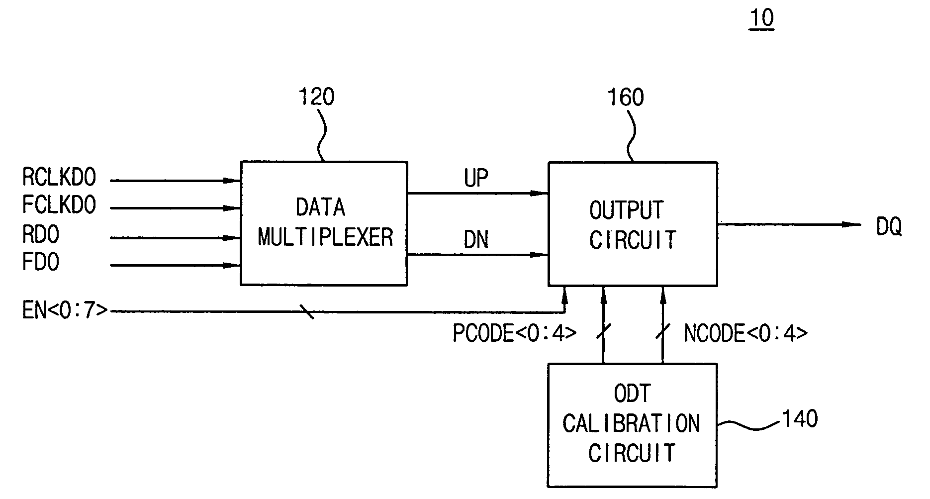
[0066]Referring to FIG. 1, a data output driver 10 according to the present invention includes a data multiplexer 120, an ODT calibration circuit 140, and an output circuit 160.
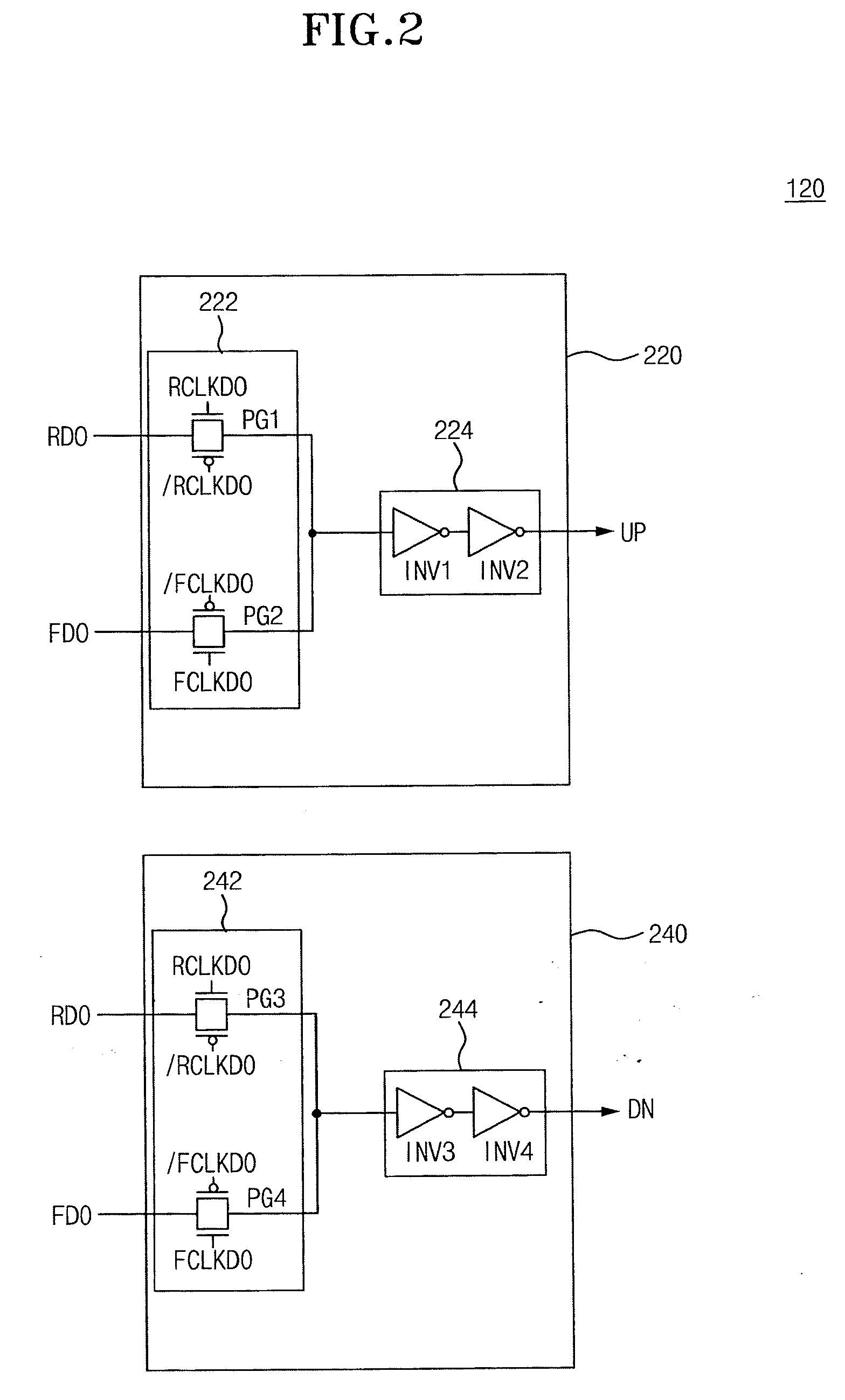
[0067]The data multiplexer 120 selectively receives an input data RDO (data synchronized at a rising edge of a clock) and an input data FDO (data synchronized at a falling edge of the clock) in response to clock signals RCLKDO (rising clock) and FCLKDO (falling clock) to output pull-up and pull-down data signals UP and DN.
[0068]The on-die termination (ODT) calibration circuit 140 performs an impedance calibration operation in proportion to a reference resistance / impedance to output pull-up and pull-down resistance-adjusting code signals PCODE and NCODE.
[0069]The output circuit 160 receives the pull-up and pull-down data signals UP and DN, the pull-up and pull-down resistance-adjusting code signals PCODE and NCODE, and an enable signal EN to generate pull-up and pull-down control signals, which are not shown i...
second embodiment
[0108]In the present invention, the finger 721 corresponding to the MSB among the fingers 721 to 725 constituting the pull-up calibration driver 720 and the finger 741 corresponding to the MSB among the fingers 741 to 745 constituting the pull-down calibration driver 740 have great strengths and thus are not used in an ODT calibration process performing fine tuning. Therefore, the ground voltage VSS is supplied to the gate of the PMOS transistor WP5, and the power voltage VDD is supplied to the gate of the NMOS transistor WN5, so that they can be always turned on. Accordingly, corresponding pull-up and pull-down resistance-adjusting code signals PCODE0> and NCODE0> are reduced to output the 4-bit pull-up and pull-down resistance-adjusting code signals PCODE and NCODE.
[0109]Referring to FIG. 8A, a second pull-up control signal generator 820 of each pull-up pre-driver includes: a driving element 830 which logic-combines the enable signal EN and the pull-up data signal UP to generate a...
third embodiment
[0118]Referring to FIG. 9, a data output driver according to the present invention includes a first multiplexer 920, a second data multiplexer 930, an ODT calibration circuit 940, and an output circuit 960.
[0119]The first data multiplexer 920 has the same structure and operation as the data multiplexer (FIG. 6) of the second embodiment. Thus, additional descriptions thereof will be omitted. The first data multiplexer 920 supplies the pull-up and pull-down data signals UP and DN to the output circuit 960.
[0120]The second data multiplexer 930 receives the input data signals RDO and FDO to output pull-up and pull-down data signals UP1 and DN1 in response to a high impedance signal H-Z generated in response to the clock signals RCLKDO, FCLKDO, and EMRS. Therefore, specific pull-up and pull-down pre-drivers receiving the pull-up and pull-down data signals UP1 and DN1 output the pull-up and pull-down control signals UPCODE and DNCODE without having to use the enable signal EN.
[0121]The OD...
PUM
 Abstract
Description
Claims
Application Information