Electrophoretic display sheet, electrophoretic display device, and electronic apparatus

a display device and display sheet technology, applied in the field of electrophoretic display devices, electrophoretic display sheets, electronic devices, can solve the problems of short circuit or damage to the circuit of thin-film transistors, degradation of electric characteristics, and uplift of electrophoretic display sheets around protection sheets, so as to prevent damage to driving circuits, superior in display quality and electric characteristics, and superior in display quality

Active Publication Date: 2008-07-03
E INK CORPORATION
View PDF5 Cites 25 Cited by
  • Summary
  • Abstract
  • Description
  • Claims
  • Application Information

AI Technical Summary

Benefits of technology

[0012]An advantage of the invention is to prevent damage to a driving circuit caused when an electrophoretic display sheet is attached to a driving substrate, and provide the electrophoretic display sheet and an electrophoretic display device superior in display quality and an electric characteristic.
[0013]As a result of dedicated investigations, the inventor of the invention found out that the electrophoretic display device superior in display quality and the electric characteristic is obtained by employing the electrophoretic display sheet while damage to the driving circuit caused when the electrophoretic display sheet is attached to the driving substrate is prevented. The electrophoretic display sheet at least includes an electrophoretic display layer; a transparent electrode layer; a transparent substrate provided with the transparent electrode layer, the transparent substrate being laminated on the electrophoretic display layer; and a stress-reducing member that reduces stress applied to the driving substrate including a semiconductor circuit layer in a case of attaching the electrophoretic display sheet to the driving substrate to be laminated with the electrophoretic display layer thereon. The invention is thus successfully completed.
[0014]The invention includes following aspects.
[0015]1) The electrophoretic display sheet at least including the electrophoretic display layer; the transparent electrode layer; the transparent substrate provided with the transparent electrode layer, the transparent substrate being laminated on the electrophoretic display layer; and the stress-reducing member that reduces stress applied to the driving substrate including the semiconductor circuit layer in a case of attaching the electrophoretic display sheet to the driving substrate to be laminated with the electrophoretic display layer thereon
[0016]2) The electrophoretic display sheet described in 1), wherein the stress-reducing member maybe an extension of an end of the transparent substrate extended to be further than an outer edge of the driving substrate, the extension coming in contact with at least a part of an upper surface of a flexible printed circuit provided on the driving substrate
[0017]3) The electrophoretic display sheet described in 1), wherein the stress-reducing member may be a buffer arranged on a lower part of an end of the transparent substrate to face to the driving substrate

Problems solved by technology

Stress caused in an attaching process makes an end of an electrophoretic display sheet dig into a driving substrate, and a transparent electrode provided on an electrophoretic display sheet comes in contact with a driving electrode, causing a short circuit or damage to a circuit of a thin-film transistor.
This thickness is larger than that of a display layer of an electrophoretic capsule (from 20 μm to 30 μm, for example), resulting in problems such as uplift of an electrophoretic display sheet around the protection sheet, and degradation of an electric characteristic.
When a soft material such as a plastic substrate is used as a rear substrate provided on a driving substrate to make an electrophoretic display flexible, aforementioned problems become even more prominent.
That is, a driving circuit is susceptible to stress because of being formed on a plastic substrate.
Therefore, a driving circuit on a plastic substrate is easily damaged by stress concentration when a driving substrate is pressed with an end of an electrophoretic display sheet to attach thereto.
However, in this case, unwanted patterns such as wiring and a driving circuit are displayed on the electrophoretic display sheet.
Further, if an end of a driving substrate is provided with an external connection terminal, unwanted patterns such as for wiring and a driving circuit are also displayed on an electrophoretic display sheet because of wiring communicating a circuit region on the driving substrate with the external connection terminal.

Method used


Image

  • Electrophoretic display sheet, electrophoretic display device, and electronic apparatus
  • Electrophoretic display sheet, electrophoretic display device, and electronic apparatus
  • Electrophoretic display sheet, electrophoretic display device, and electronic apparatus

Examples


first embodiment

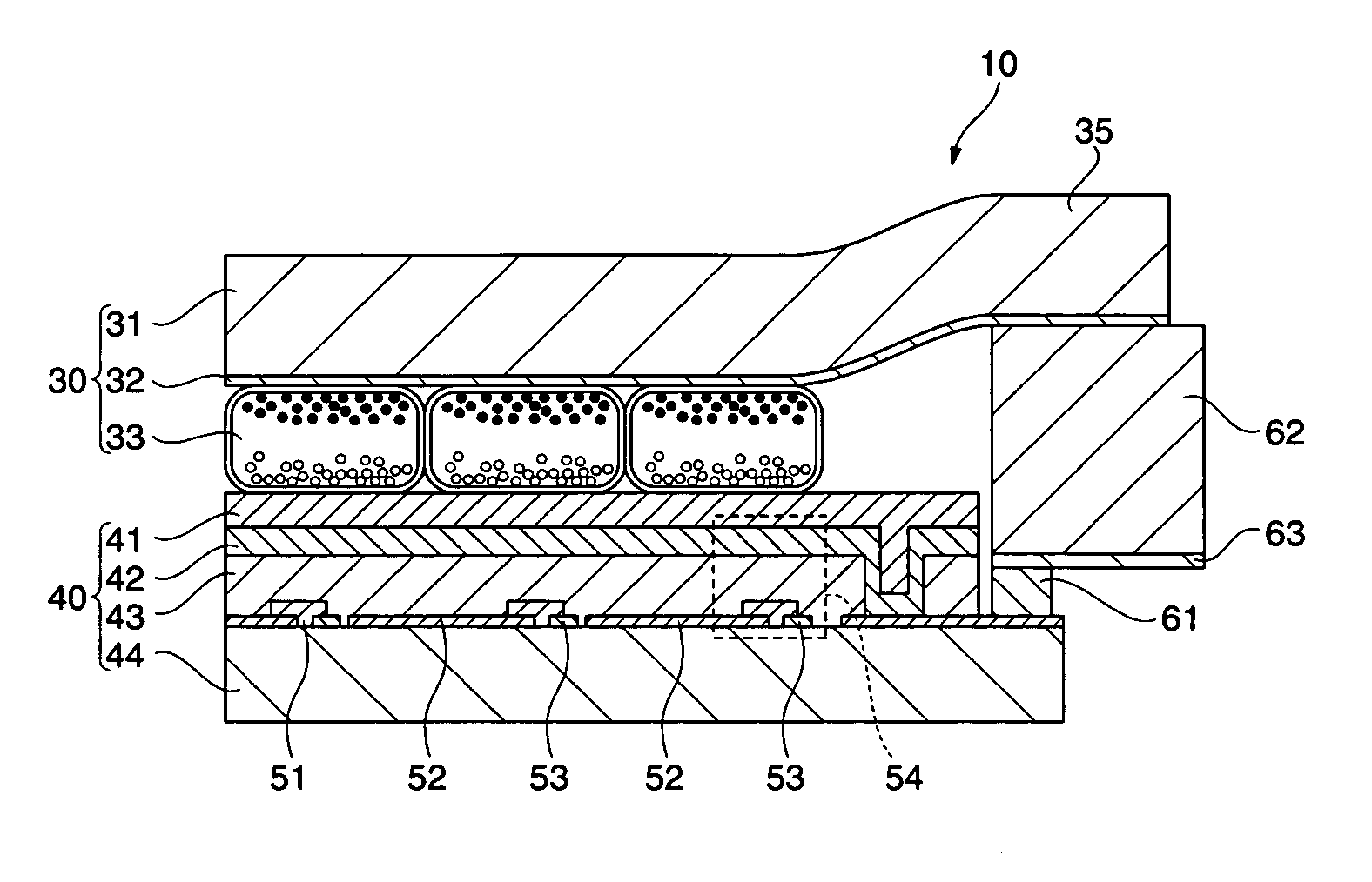
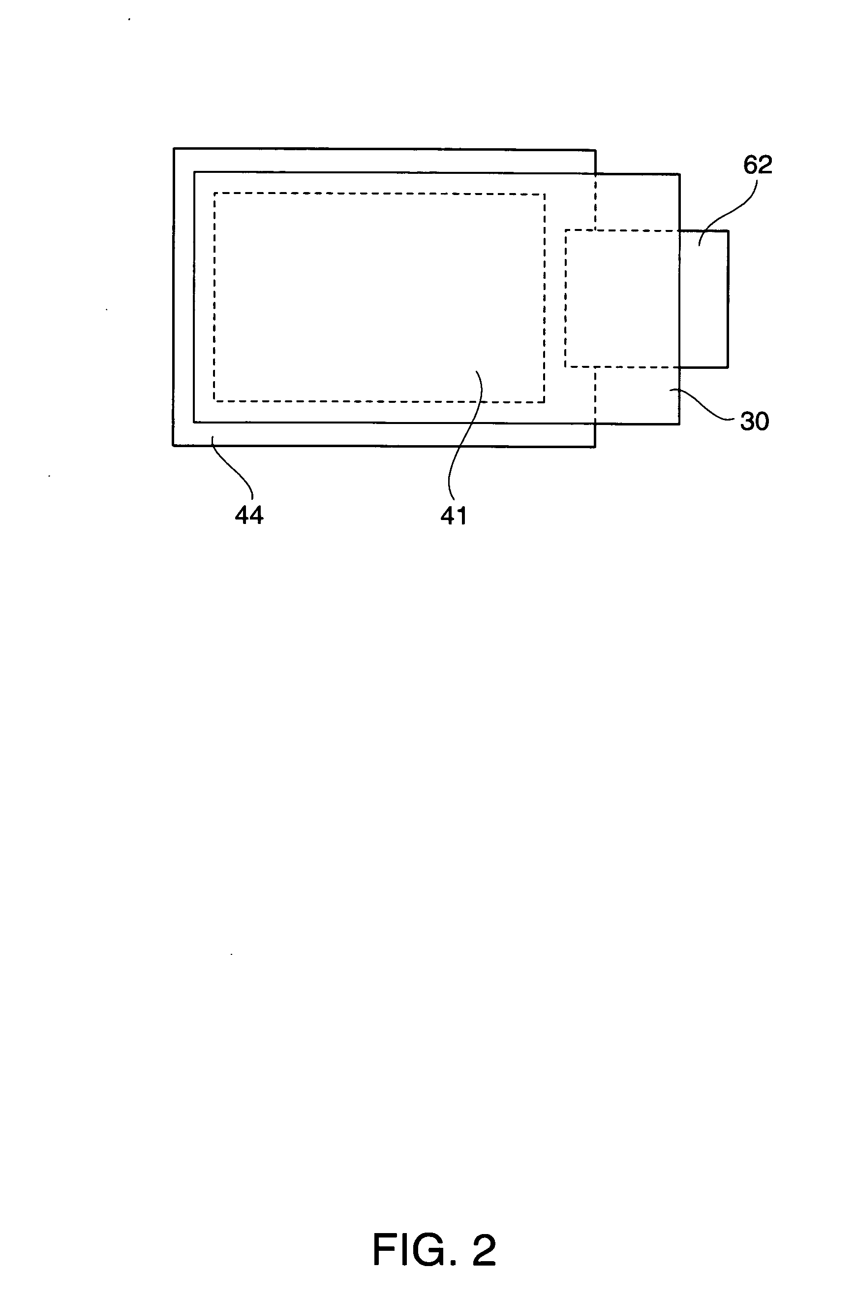
[0044]FIG. 1 is a sectional view showing a part of an electrophoretic display device 10 while FIG. 2 is an overhead view of the electrophoretic display device 10 according to a first embodiment.

[0045]As shown in FIGS. 1 and 2, the electrophoretic display device 10 includes an electrophoretic display sheet 30 and a driving substrate 40. It is preferably that the electrophoretic display device 10 be formed by laminating the electrophoretic display sheet 30 having flexibility on the driving substrate 40 having flexibility.

[0046]The electrophoretic display sheet 30 includes an electrophoretic display layer 33 and a transparent substrate 31 laminated on the electrophoretic display layer 33 and having a transparent electrode 32 on the undersurface thereof. The transparent substrate 31 is made of a transparent insulating binder resin such as a polyethylene terephthalate (PET) film. The transparent electrode layer 32 is an indium tin oxide film (ITO film) having tin doped in.

[0047]The elect...

second embodiment

[0058]FIG. 3 is a sectional view showing a part of an electrophoretic display device 11 according to a second embodiment.

[0059]As shown in FIG. 3, the electrophoretic display device 11 in the second embodiment has a buffer 37 instead of the extension 35. This is the only difference between the first embodiment and the second embodiment. Like numbers refer to like parts in FIGS. 1 and 3, and the description thereof is omitted here.

[0060]The buffer 37 is arranged underneath the end of the transparent substrate 31 provided with the transparent electrode layer 32 to face to the driving substrate 40.

[0061]In the second embodiment, the end of the transparent substrate 31 is also prevented from coming in contact with the driving substrate 40. That is, stress on the driving substrate 40 caused when the electrophoretic display sheet 30 is attached to the driving substrate 40 is reduced, providing an electrophoretic display sheet and an electrophoretic display device superior in display quali...

third embodiment

[0062]FIG. 4A is a sectional view showing a part of an electrophoretic display device 12 in a third embodiment. FIG. 4B is a diagram showing a state in which a protection sheet 39, the flexible printed circuit 62, and the anisotropic conductive film 63 are integrated before assembly. FIG. 5 is an overhead view of the electrophoretic display device 12.

[0063]As shown in FIGS. 4A, 4B, and 5, the electrophoretic display device 12 in the third embodiment has the protection sheet 39 instead of the extension 35. This is the only difference between the first embodiment and the third embodiment. As shown in FIG. 4B, an end of the protection sheet 39 is bonded onto the flexible printed circuit 62 provided on the driving substrate 40 to be preliminarily integrated.

[0064]As shown in FIG. 4A, by assembling a unit which is integrated as shown in FIG. 4B, the end of the protection sheet 39 is arranged between the driving substrate 40 and the transparent substrate 31 provided with the transparent e...


PUM

PropertyMeasurementUnit
thicknessaaaaaaaaaa
thicknessaaaaaaaaaa
thicknessaaaaaaaaaa

Abstract

An electrophoretic display sheet includes an electrophoretic display layer; a transparent electrode layer; a transparent substrate provided with the transparent electrode layer, the transparent substrate being laminated on the electrophoretic display layer; and a stress-reducing member that reduces stress applied to a driving substrate including a semiconductor circuit layer in a case of attaching the electrophoretic display sheet to the driving substrate to be laminated with the electrophoretic display layer thereon.

Description

BACKGROUND[0001]1. Technical Field[0002]An aspect of the present invention relates to an electrophoretic display sheet, an electrophoretic display device, and an electronic apparatus using electrophoretic migration in which charged particles in a medium migrate by applying a voltage to form images, in particular, an electrophoretic display device, and an electronic apparatus enabling to avoid damage to a driving circuit by reducing stress applied to a driving substrate when an electrophoretic display sheet is attached to the driving substrate.[0003]2. Related Art[0004]An electrophoretic display device (so-called EPD display device) provided with an electrophoretic element is a display device using electrophoretic migration in which particles dispersed in a solvent migrate by applying a voltage. As for methods for electrophoretic migration, for example, a microcapsule type, a horizontal migration type, and a vertical type have been developed. EPD display devices are easily processed ...

Claims


Application Information

Patent Timeline
Patent Type & Authority Applications(United States)
IPC IPC(8): G02B26/00G02F1/167
CPCG02F1/133305G02F2201/503G02F1/167G02F1/1362
Inventor KAWASE, TAKEOYAMAMOTO, HITOSHISAEKI, TAKEHISAMIYAMOTO, TSUTOMU
Owner E INK CORPORATION
Why Eureka
Try Eureka